Light-emitting device, method for manufacturing light-emitting device, and electronic apparatus

a technology of light-emitting devices and electronic devices, which is applied in the direction of discharge tubes/lamp details, luminescent screens, transportation and packaging, etc., can solve the problems of reducing life, affecting the effect of light-emitting device performance, and affecting the quality of light-emitting devices, so as to prevent moisture penetration and/or oxygen penetration, the effect of easy damage or crack

Active Publication Date: 2006-07-20
SEIKO EPSON CORP
View PDF18 Cites 96 Cited by
  • Summary
  • Abstract
  • Description
  • Claims
  • Application Information

AI Technical Summary

Benefits of technology

[0010] An advantage of the invention is that it provides light-emitting devices in which the penetration of moisture can be prevented if a gas barrier layer is chipped or cracked, a method for manufacturing a light-emitting device, and an electronic apparatus including a light-emitting device.
[0011] The invention provides light-emitting devices, a method for manufacturing a light-emitting device, and an electronic apparatus including a light-emitting device.
[0012] A light-emitting device according to the invention includes a base; a plurality of first electrodes; a partition having a plurality of openings located at positions corresponding to the first electrodes; organic functional layers each arranged in the corresponding openings; a second electrode covering the partition and the organic functional layers; an organic buffer layer covering the second electrode; a gas barrier layer covering the organic buffer layer; and an intermediate protective layer, disposed between the organic buffer layer and the gas barrier layer, having an elasticity which is greater than that of the organic buffer layer and which is less than that of the gas barrier layer. These layers and electrodes are arranged on or above the base.
[0013] According to the light-emitting device, since the intermediate protective layer is disposed between the organic buffer layer and the gas barrier layer, the thermal distortion (expansion or shrinkage) of the organic buffer layer is not directly transmitted to the gas barrier layer; hence, the gas barrier layers can be prevented from being damaged or cracked. In particular, although the gas barrier layer covering an end face of the organic buffer layer is easily damaged or cracked, the creation of defects such as cracks in the gas barrier layer can be effectively prevented by the presence of the intermediate protective layer.
[0014] In the light-emitting device, the intermediate protective layer preferably covers an outer region of the organic buffer layer. The intermediate protective layer prevents the creation of defects such as cracks in the gas barrier layer.
[0015] The intermediate protective layer preferably extends over a pattern of the organic buffer layer and a region outside the organic buffer layer. The intermediate protective layer prevents moisture from penetrating the organic buffer layer.

Problems solved by technology

Most of materials for forming light-emitting layers, hole injection layers, and electron injection layers included in organic electroluminescent devices are usually deteriorated by the reaction with moisture in air.
This leads to a reduction in life.
In the organic electroluminescent devices, it is a challenge to prevent damage caused by moisture, oxygen, or the like.
However, in large-screen displays having low thickness and weight, it is difficult to prevent the penetration of moisture and / or oxygen using only sealing members.
However, even if this technique is used, the penetration of external moisture cannot be completely prevented; hence, sufficient luminescent properties and life cannot be achieved.
In particular, steps present around the gas barrier layer or present on partitions for partitioning pixels are easily chipped or cracked and moisture penetrates the chipped or cracked steps.
However, if the organic buffer layer is thermally distorted (expanded or shrunk), the gas barrier layer is cracked.
Therefore, there is a problem in that the penetration of external moisture cannot be completely prevented.

Method used


Image

  • Light-emitting device, method for manufacturing light-emitting device, and electronic apparatus
  • Light-emitting device, method for manufacturing light-emitting device, and electronic apparatus
  • Light-emitting device, method for manufacturing light-emitting device, and electronic apparatus

Examples


first embodiment

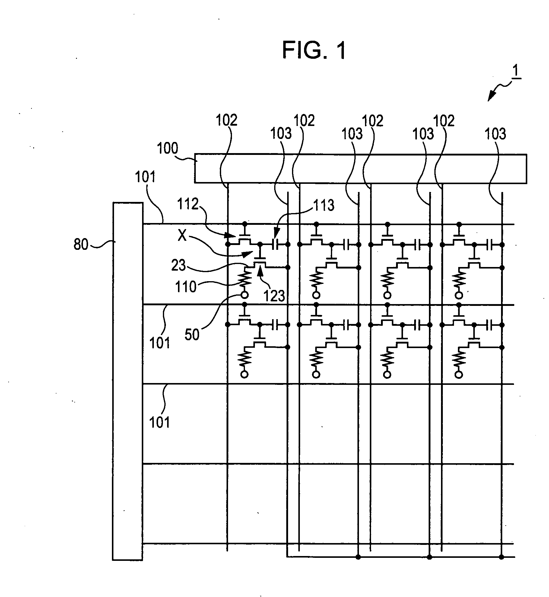
[0061]FIG. 1 is a wiring diagram of an EL display device (a light-emitting device) 1 according to a first embodiment of the invention.

[0062] The EL display device 1 includes thin-film transistors (hereinafter simply referred to as TFTs) serving as switching elements and is of an active matrix type.

[0063] In the drawings, in order to show layers and members included in the EL display device 1 on a recognizable scale, different scales are used depending on the size of the layers and members.

[0064] With reference to FIG. 1, the EL display device 1 includes a plurality of scanning lines 101, a plurality of signal lines 102 extending orthogonally to the scanning line 101, a plurality of power supply lines 103 extending parallel to the signal lines 102, pixel regions X located near the intersections of the scanning lines 101 and signal lines 102.

[0065] The signal lines 102 are connected to a data line-driving circuit 100 including a shift register, a level shifter, video lines, and an...

second embodiment

[0191] An EL display device 2 according to a second embodiment of the invention will now be described. In this embodiment, the same components as those described in the first embodiment have the same reference numerals as those described in the first embodiment in order to omit the descriptions thereof.

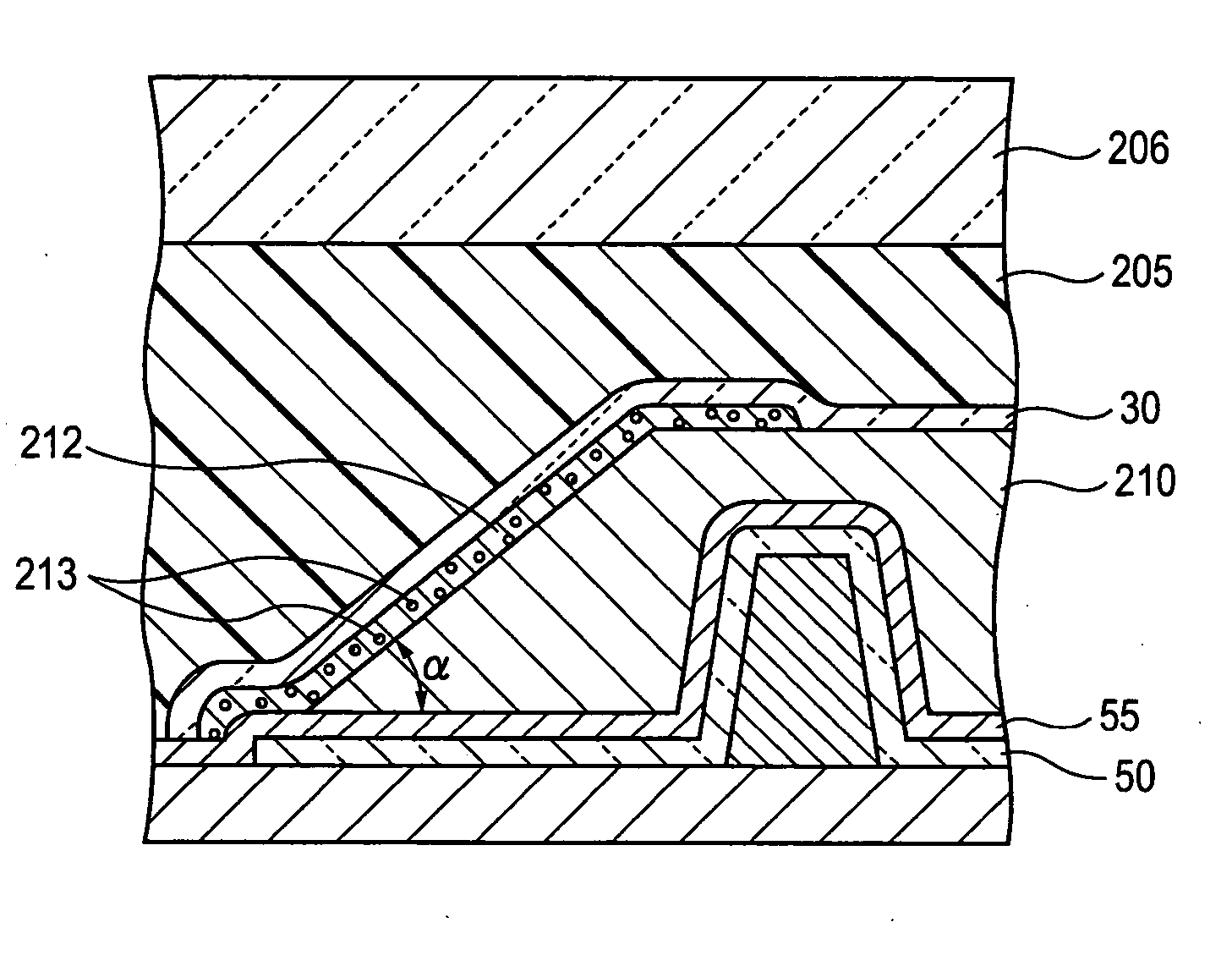
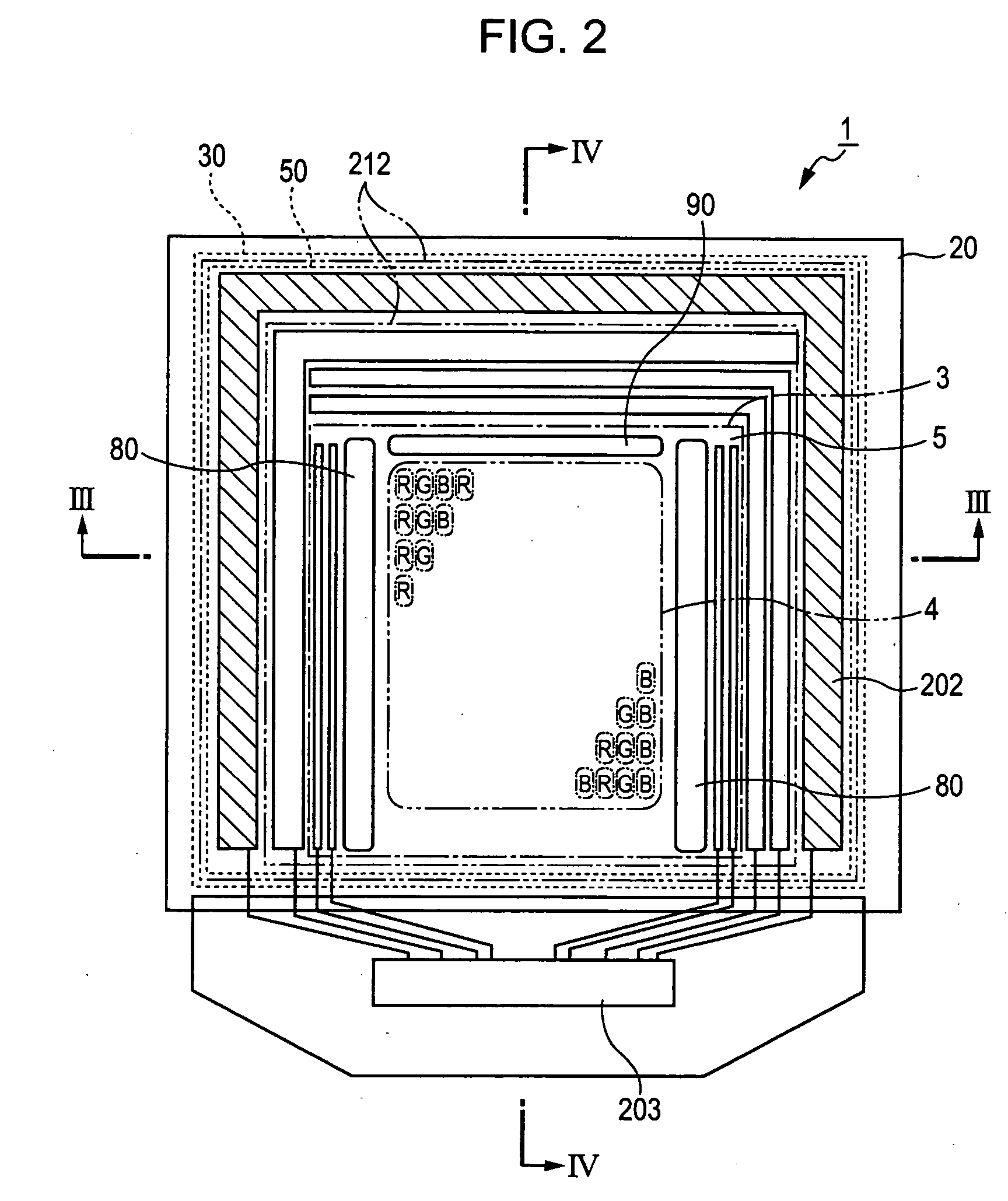
[0192]FIG. 11 is a schematic sectional view of the EL display device 2. FIG. 12 is an enlarged view of an end portion (an outer region) of an organic buffer layer 210 included in the EL display device 2.

[0193] The EL display device 2 is different from the EL display device 1 of the first embodiment in that the EL display device 2 includes white light-emitting layers 60W and a color filter substrate 207 serving as a surface protection substrate.

[0194] The white light-emitting layers 60W are made of a white organic luminescent material such as a styrylamine-based luminescent material, an anthracene-based dopant (blue), or a rubrene-based dopant (yellow).

[0195] The following layers a...

examples

[0209] Problems caused in EL display devices will now be described. The EL display devices include organic buffer layers 210, gas barrier layers 30, and intermediate protective layers 212 each disposed therebetween.

[0210]FIG. 13 is a table showing the problems.

[0211] The EL display devices, including the intermediate protective layer 212 made of various materials, similar to the above EL display devices 1 and 2 were prepared and then subjected to a thermal cycle test or a high-humidity test. The EL display devices were evaluated if the gas barrier layers 30 had end portions (outer regions) penetrated by moisture.

[0212] The EL display devices included pixel electrodes 23 with a thickness of 100 nm; white light-emitting layers 60W with a thickness of 150 nm; cathodes 50 with a thickness of 15 nm; cathode-protecting layers 55, made of SiON, having a thickness of 100 μm; and protective layers 204 with a thickness of 100 μm. The organic buffer layers 210 had a thickness of 5 μm and th...


PUM


Abstract

A light-emitting device includes a base; a plurality of first electrodes; a partition having a plurality of openings located at positions corresponding to the first electrodes; organic functional layers each arranged in the corresponding openings; a second electrode covering the partition and the organic functional layers; an organic buffer layer covering the second electrode; a gas barrier layer covering the organic buffer layer; and an intermediate protective layer, disposed between the organic buffer layer and the gas barrier layer, having an elasticity which is greater than that of the organic buffer layer and which is less than that of the gas barrier layer. These layers and electrodes are arranged on or above the base.

Description

CROSS-REFERENCE TO RELATED APPLICATIONS [0001] The present application claims priority to Japanese Patent Application No. 2005-008695 filed on Jan. 17, 2005 in Japan and Japanese Patent Application No. 2005-353028 filed on Dec. 7, 2005 in Japan, which are hereby expressly incorporated by reference herein in their entirety. BACKGROUND [0002] The present invention relates to a light-emitting device, a method for manufacturing the light-emitting device, and an electronic apparatus including the light-emitting device. [0003] In recent years, flat-panel displays which have low power consumption and which are lightweight have been demanded since various information apparatuses incorporating the displays have been developed. An organic electroluminescent device including light-emitting layers is known as an example of such flat-panel displays. In the organic electroluminescent device, the light-emitting layers are usually arranged between a cathode and anodes. In order to enhance the hole ...

Claims


Application Information

Patent Timeline
Patent Type & Authority Applications(United States)
IPC IPC(8): H01L51/52H05B33/02
CPCH01L27/3244Y10T428/24942H01L51/5237H01L27/3295H10K59/88H10K59/122H10K59/12H10K50/8426H10K50/846H10K50/844H05B33/00
Inventor HAYASHI, KENJI
Owner SEIKO EPSON CORP
Why Eureka
Try Eureka