Semiconductor device capable of preventing moisture-absorption of fuse area thereof and method for manufacturing the fuse area

a technology of a semiconductor device and a fuse area, which is applied in the direction of semiconductor devices, semiconductor/solid-state device details, electrical equipment, etc., can solve the problems of affecting the reliability of semiconductor devices, affecting the cutting efficiency of fuse blades, and unable to withstand much moisture, so as to reduce the increase in the layout area, reduce the effect of moisture permeation and reduce the increase of the layout area

Inactive Publication Date: 2005-10-06
SAMSUNG ELECTRONICS CO LTD
View PDF11 Cites 17 Cited by
  • Summary
  • Abstract
  • Description
  • Claims
  • Application Information

AI Technical Summary

Benefits of technology

[0012] To solve the above problems, it is a first object of the present invention to provide a semiconductor device having a fuse area better protected at preventing moisture-permeation and allowing for efficient cutting of fuses.
[0013] It is a second object of the present invention to provide a method for forming a fuse area of a semiconductor device, which is better at preventing moisture-absorption and allows for efficient cutting of fuses.
[0021] According to the present invention, the guard ring is formed at one time using the passivation layer or the uppermost wiring, thereby efficiently preventing permeation of moisture through the interface between the interlayer insulating films.
[0022] In addition, when the guard ring is simultaneously formed with the uppermost interconnect wiring, the passivation layer is etched to expose the part of the guard ring when forming the fuse opening portion, thereby minimizing an increase in a layout area due to formation of the guard ring.
[0023] Moreover, according to an embodiment of the present invention, the etch stop layer is used when an etching process is performed for forming the fuse opening portion so that the thickness of an interlayer insulating film remaining on the fuse line can be accurately controlled as compared with a conventional method of forming a fuse opening portion using timed etching, thereby improving the cutting efficiency of a fuse.

Problems solved by technology

However, films containing a large amount of impurity, such as the above described BPSG film, PSG film, SOG film and TEOS film, in which boron (B) exceeds 5 weight percent and phosphorous (P) exceeds 4 weight percent, cannot withstand much moisture.
As a result, metal interconnects, for example, the interconnect wirings 38 and 42 formed of aluminum, corrode, thereby degrading the reliability of semiconductor devices.

Method used


Image

  • Semiconductor device capable of preventing moisture-absorption of fuse area thereof and method for manufacturing the fuse area
  • Semiconductor device capable of preventing moisture-absorption of fuse area thereof and method for manufacturing the fuse area
  • Semiconductor device capable of preventing moisture-absorption of fuse area thereof and method for manufacturing the fuse area

Examples


Embodiment Construction

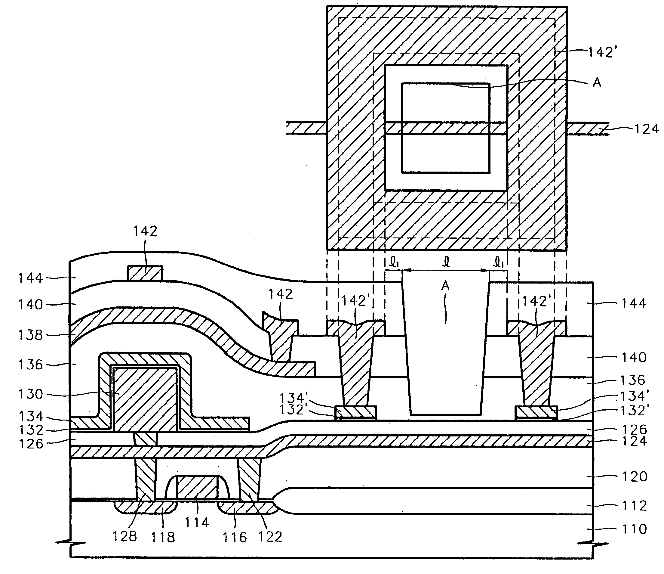
[0030] A portion of a DRAM device is illustrated in FIGS. 3 through 7. FIG. 3 shows a capacitor (130, 132, and 134). A fuse area in this embodiment is concurrently formed with a cell array area. Using conventional techniques, a device isolation film 112 is formed on a substrate 110. Then, a gate electrode 114 and source and drain regions 118 and 116 of a transistor are formed. An interlayer insulating film 120 is deposited on the entire surface of the substrate 110 including the device isolation film 112. Subsequently, the interlayer insulating film 120 is etched to form a contact hole exposing the drain region 116. Next, a conductive material, for example, doped polysilicon, metal silicide or a stacked film of polysilicon and metal silicide, is processed conventionally to form a contact plug 122 in the contact hole and a bit line 124 extending across the region of the device. The bit line 124 on the right of FIG. 3 functions as a fuse line. As described above, instead of the bit li...


PUM


Abstract

A fuse area of a semiconductor device capable of preventing moisture-absorption and a method for manufacturing the fuse area are provided. When forming a guard ring for preventing permeation of moisture through the sidewall of an exposed fuse opening portion, an etch stop layer is formed over a fuse line. A guard ring opening portion is formed using the etch stop layer. The guard ring opening portion is filled with a material for forming the uppermost wiring of multi-level interconnect wirings or the material of a passivation layer, thereby forming the guard ring concurrently with the uppermost interconnect wiring or the passivation layer. Accordingly, permeation of moisture through an interlayer insulating layer or the interface between interlayer insulating layers around the fuse opening portion can be efficiently prevented by a simple process. In addition, the etch stop layer is also formed under the fuse opening portion so that an insulating layer remaining on the fuse line can be controlled to have a predetermined thickness when forming the fuse opening portion, thereby improving the cutting efficiency of fuses.

Description

[0001] This application is a Divisional of U.S. Ser. No. 10 / 334,745, filed on Dec. 31, 2002, now pending, which is a divisional of U.S. patent application Ser. No. 09 / 650,967, filed on Aug. 29, 2000, now issued U.S. Pat. No. 6,525,398, which claims priority from Korean Patent Application No. 1999-36534, filed on Aug. 31, 1999, all of which are hereby incorporated by reference in their entirety.BACKGROUND OF THE INVENTION [0002] 1. Field of the Invention [0003] The present invention relates to a semiconductor device and a method for manufacturing the same, and more particularly, to the structure of a fuse area and a method for forming the fuse area. [0004] 2. Description of the Related Art [0005] Generally, semiconductor devices are formed by stacking material layers of various patterns and finally depositing a protection film called a passivation film. The passivation film, conventionally formed of a hard film such as a silicon nitride film, protects semiconductor devices, especiall...

Claims


Application Information

Patent Timeline
Patent Type & Authority Applications(United States)
IPC IPC(8): H01L21/768H01L27/00H01L21/82H01L21/8242H01L21/8244H01L23/00H01L23/525H01L23/58H01L27/108
CPCH01L21/768H01L23/5258H01L23/564H01L23/585H01L27/10814H01L27/10894H01L27/11H01L2924/0002Y10S257/908Y10S257/906Y10S257/907H01L2924/00H10B12/315H10B12/09H10B10/00H01L27/00
Inventor KIM, BYUNG-YOONLEE, WON-SEONGPARK, YOUNG-WOO
Owner SAMSUNG ELECTRONICS CO LTD
Why Eureka
Try Eureka