Circuit structure and manufacturing method thereof

a technology of circuit structure and manufacturing method, applied in the field of circuit structure, can solve the problems of deterioration of electrical quality of circuit boards, inability to manage the etching rate, etc., and achieve the effect of preventing galvanic effects

US20120282738A1Active Publication Date: 2012-11-08SUBTRON TECH
1 Cites 3 Cited by

Patent Information

Authority / Receiving Office
US · United States
Current Assignee / Owner
Publication Date
2012-11-08

Smart Images

  • Figure 1
    Figure 1
  • Figure 2
    Figure 2
Patent Text Reader

Abstract

A manufacturing method of a circuit structure is provided. A metal layer having an upper surface is provided. A surface passivation layer is formed on the metal layer. The surface passivation layer exposes a portion of the upper surface of the metal layer, and a material of the metal layer is different from a material of the surface passivation layer. The metal layer and the surface passivation layer are dipped into a modifier, and the modifier is selectively absorbed and attached to the surface passivation layer, so as to form a covering layer. The covering layer has a plurality of nanoparticles and covers the surface passivation layer.
Need to check novelty before this filing date? Find Prior Art

Description

CROSS-REFERENCE TO RELATED APPLICATION

[0001] This application claims the priority benefit of Taiwan application serial no. 100115619, filed May 4, 2011. The entirety of the above-mentioned patent application is hereby incorporated by reference herein and made a part of this specification.BACKGROUND OF THE INVENTION

[0002] 1. Field of the Invention

[0003] The invention relates to a circuit structure and a manufacturing method thereof. More particularly, the invention relates to a circuit structure capable of preventing Galvanic effects from occurring in an etching process or in any process that can lead to electrochemical reaction and a manufacturing method of the circuit structure.

[0004] 2. Description of the Related Art

[0005] Circuit boards applied in the existing semiconductor package process have advantages of closed wiring, compact assembly, and favorable performance, the circuit boards have become one of the most applicable package devices. A circuit board can be assembled to a plural...

Examples

Embodiment Construction

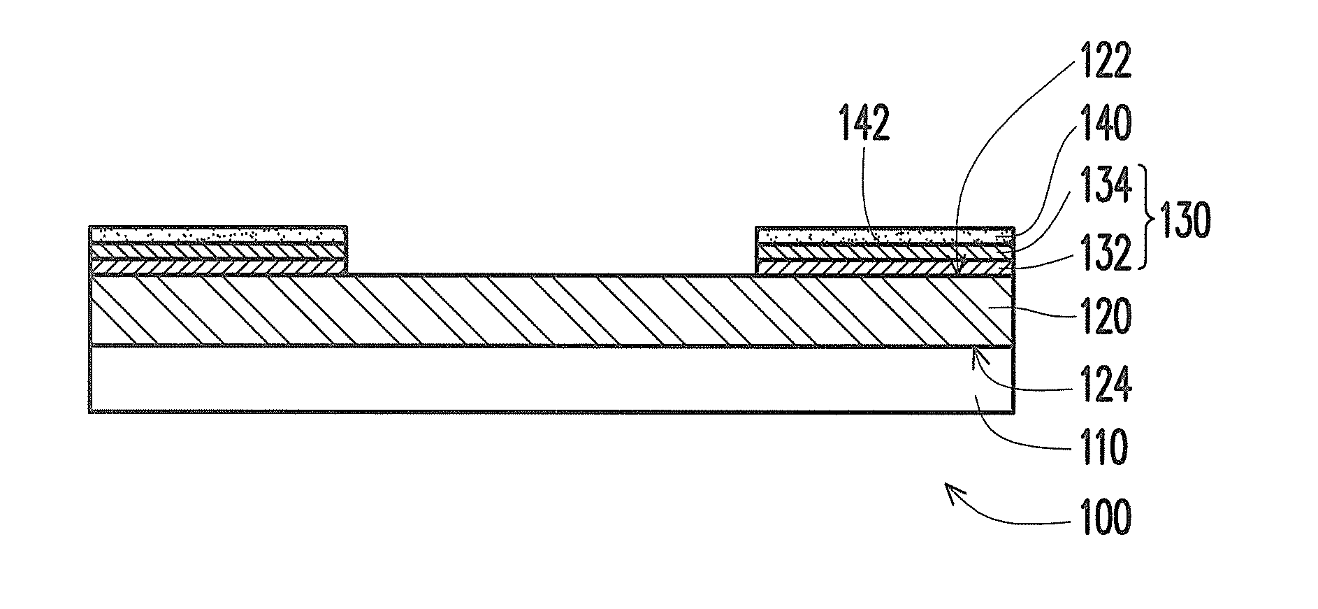
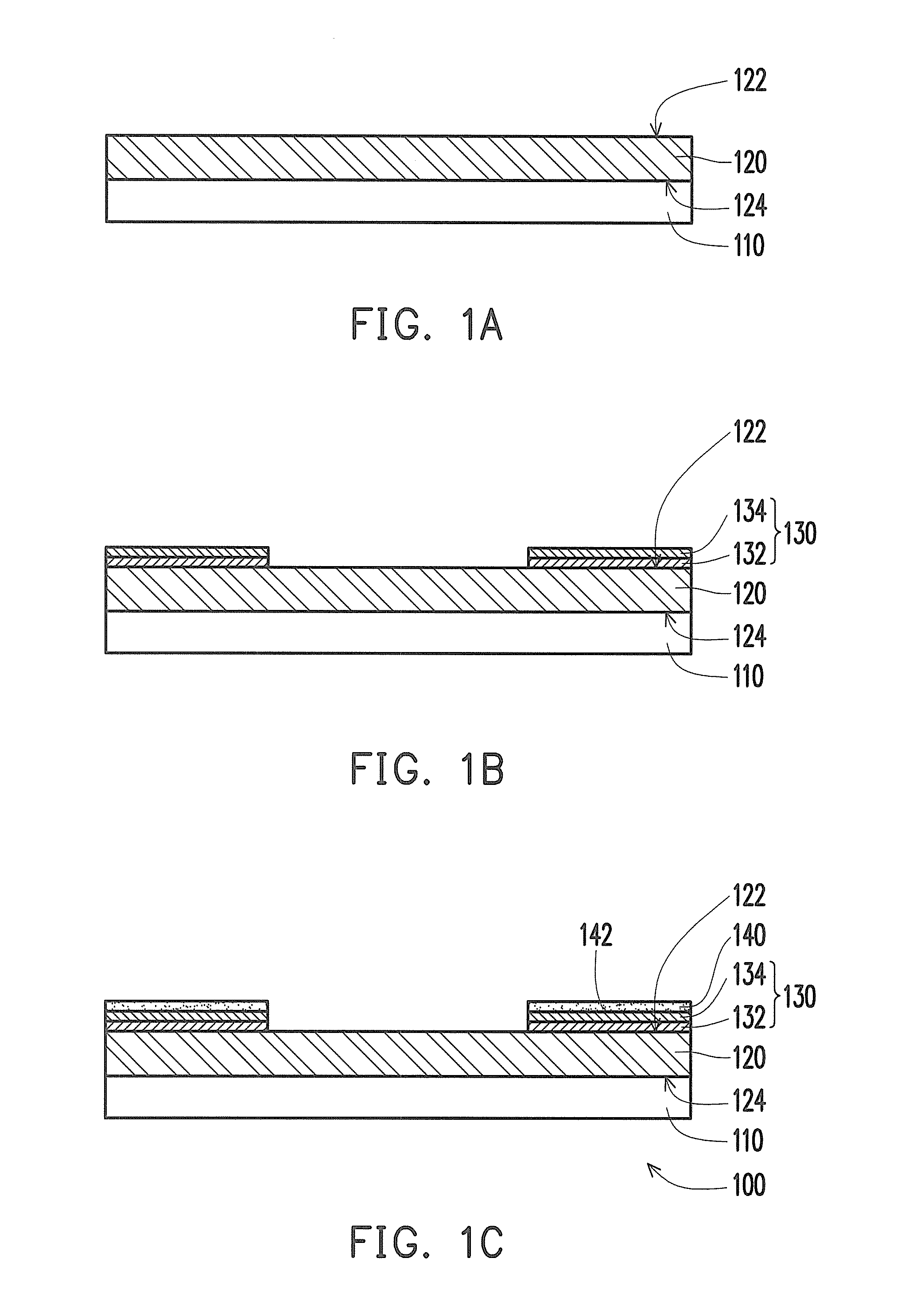
[0028]FIG. 1A to FIG. 1C are cross-sectional views illustrating a manufacturing method of a circuit structure according to an embodiment of the invention. With reference to FIG. 1A, in the manufacturing method of the circuit structure of this embodiment, an insulation layer 110 and a metal layer 120 are provided. The metal layer 120 has an upper surface 122 and a lower surface 124 opposite to the upper surface 122. The insulation layer 110 is configured on the lower surface 124 of the metal layer 120, so as to support the metal layer 120. According to this embodiment, the metal layer 120 is made of copper or a copper alloy, for instance.

[0029]With reference to FIG. 1B, a surface passivation layer 130 is formed on the metal layer 120. The surface passivation layer 130 exposes a portion of the upper surface 122 of the metal layer 120, and a material of the metal layer 120 is different from a material of the surface passivation layer 130. The surface passivation layer 130 of this embod...