Fabricating process of circuit board with embedded passive component

a technology of passive components and circuit boards, applied in the direction of printed resistor incorporation, printed capacitor incorporation, non-metallic protective coating applications, etc., can solve the problem of more evident resistance capacitance delay or cross talk effect, and the passive component with specific electrical values may not completely satisfy the electrical quality

Inactive Publication Date: 2009-06-04
SUBTRON TECH
View PDF0 Cites 3 Cited by
  • Summary
  • Abstract
  • Description
  • Claims
  • Application Information

AI Technical Summary

Benefits of technology

[0008]The present invention is directed to a fabricating process of a circuit board with an embedded passive compone...

Problems solved by technology

However, as the layer number of the circuit boards and the integration of circuits increase, the electrical signals transmitted in the circuit board cause more evident Resistance Capacitance delay or cross talk eff...

Method used


Image

  • Fabricating process of circuit board with embedded passive component
  • Fabricating process of circuit board with embedded passive component
  • Fabricating process of circuit board with embedded passive component

Examples


first embodiment

The First Embodiment

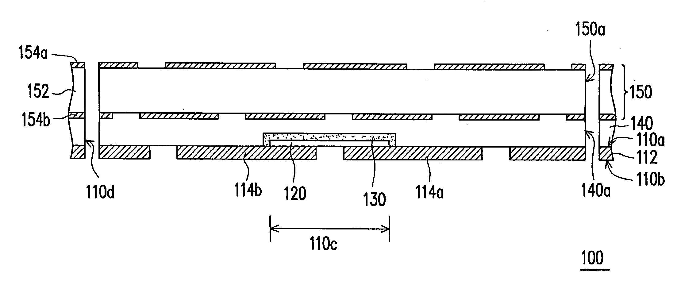
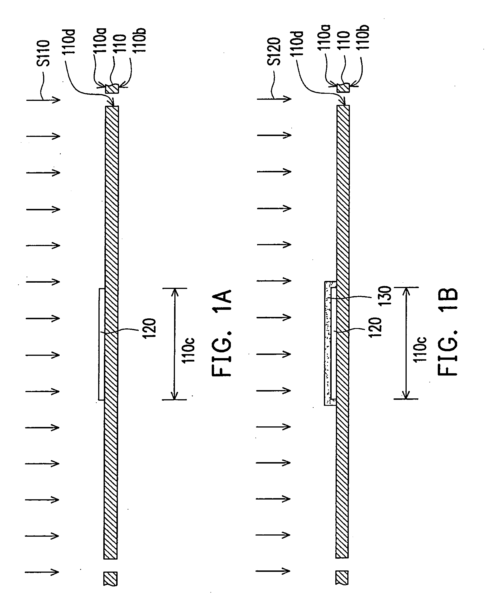
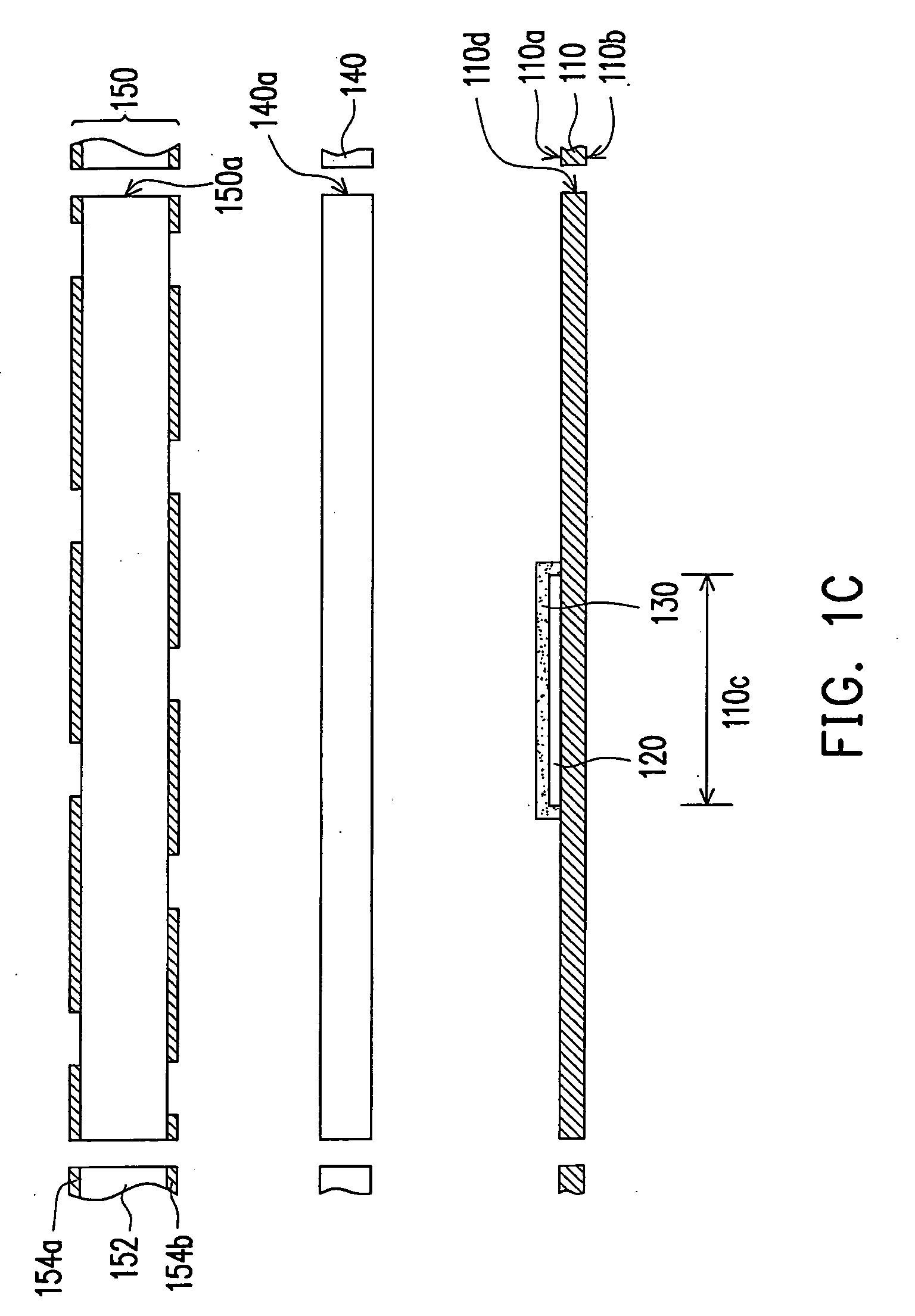
[0031]FIGS. 1A to 1D are the schematic cross-sectional views illustrating a fabricating process of a circuit board with an embedded passive component according to the first embodiment of the present invention. Referring to FIG. 1A, according to the present embodiment, the fabricating process of the circuit board with the embedded passive component includes the following steps: First, a conductive layer 110 is provided and the conductive layer 110 includes a first surface 110a and a second surface 110b opposite thereto, wherein the first surface 110a can have at least one component region 110c, and the conductive layer 110 can be a copper foil layer. In addition, according to the present embodiment, in order to facilitate the alignment of the conductive layer 110 in the following steps, the fabricating process of the circuit board can also include forming a plurality of first through holes 110d in the conductive layer 110, and a method of forming the first through...

second embodiment

[0038]FIGS. 2A to 2D are the schematic cross-sectional views illustrating a fabricating process of a circuit board with an embedded passive component according to the second embodiment of the present invention. Referring to FIG. 2A, the present embodiment is similar to the first embodiment with the difference lying in that the present embodiment of the fabricating process of the circuit board with the embedded passive component includes forming at least one electrode layer 210 on the passive component material layer 120 and the component region 110c after forming the passive component material 120. In addition, the electrode layer 210 can be made of copper paste, and the method of forming the electrode layer 210 can be screen printing. Then, a curing process is performed to cure the electrode layer 210. Then, as in the first embodiment, a plasma treatment S110 is performed to the conductive layer 110, the passive component material layer 120 and the electrode layer 210 in order to e...


PUM

PropertyMeasurementUnit
Electrical resistanceaaaaaaaaaa
Electrical inductanceaaaaaaaaaa
Electrical conductoraaaaaaaaaa

Abstract

A fabricating process of a circuit board with an embedded passive component is described. First, a conductive layer including a first surface and a second surface opposite thereto is provided. The first surface has at least one component region on which at least one passive component material layer is formed. A passivation layer is formed on the first surface to cover the passive component material layer. A brown oxidation process is performed on the conductive layer. A circuit unit and an insulation layer are provided, and the insulation layer is set between the circuit unit and the conductive layer. The conductive layer, the circuit unit and the insulation layer are laminated. The passive component material layer is between the insulation layer and the conductive layer. The conductive layer is patterned to form a circuit layer.

Description

CROSS-REFERENCE TO RELATED APPLICATION[0001]This application claims the priority benefit of Taiwan application serial no. 96145911, filed on Dec. 3, 2007. The entirety of the above-mentioned patent application is hereby incorporated by reference herein and made a part of this specification.BACKGROUND OF THE INVENTION[0002]1. Field of the Invention[0003]The present invention relates to a fabricating process of a circuit board, and in particular to a fabricating process of a circuit board with an embedded passive component.[0004]2. Description of Related Art[0005]As the integration of electronic products is increasingly improved, circuit layers of a circuit board applied to the high-integration electronic products increase from single layer, double layer to 6 layers, 8 layers and even more than 10 layers, so as to mount more electronic components on the printed circuit board. However, as the layer number of the circuit boards and the integration of circuits increase, the electrical si...

Claims


Application Information

Patent Timeline
IPC IPC(8): H05K1/16H05K3/30
CPCH05K1/162H05K1/165H05K1/167H05K3/28H05K3/385Y10T29/4913H05K2201/0187H05K2201/0355H05K2201/09763H05K2203/0315H05K2203/095H05K3/4652
Inventor LEE, YING-MING
Owner SUBTRON TECH
Why Eureka
Try Eureka