Process for manufacturing an interaction structure for a storage medium

a technology of interaction structure and storage medium, which is applied in the field of process for manufacturing interaction structure for storage medium, can solve the problems of major limitations of storage system using magnetism-based technology, increase in data-storage capacity, read/write speed and size reduction,

Active Publication Date: 2009-04-16
STMICROELECTRONICS SRL
View PDF12 Cites 6 Cited by
  • Summary
  • Abstract
  • Description
  • Claims
  • Application Information

AI Technical Summary

Benefits of technology

[0010]One embodiment is a manufacturing process that enables the aforesaid problems and disadvantages to be overcome, and in particular that enables definition of an interaction head of nanometric dimensions without resorting to the use of a purely lithographic process.

Problems solved by technology

As is known, storage systems using a magnetism-based technology, such as, for example, hard disks, suffer from major limitations as regards the increase in data-storage capacity, the read / write speed, and size reduction.
In particular, in the case where ferroelectric storage media are used, the read operations are destructive, i.e., they imply removal of the stored information and the impossibility for carrying out any subsequent reading of the same data.

Method used


Image

  • Process for manufacturing an interaction structure for a storage medium
  • Process for manufacturing an interaction structure for a storage medium
  • Process for manufacturing an interaction structure for a storage medium

Examples


first embodiment

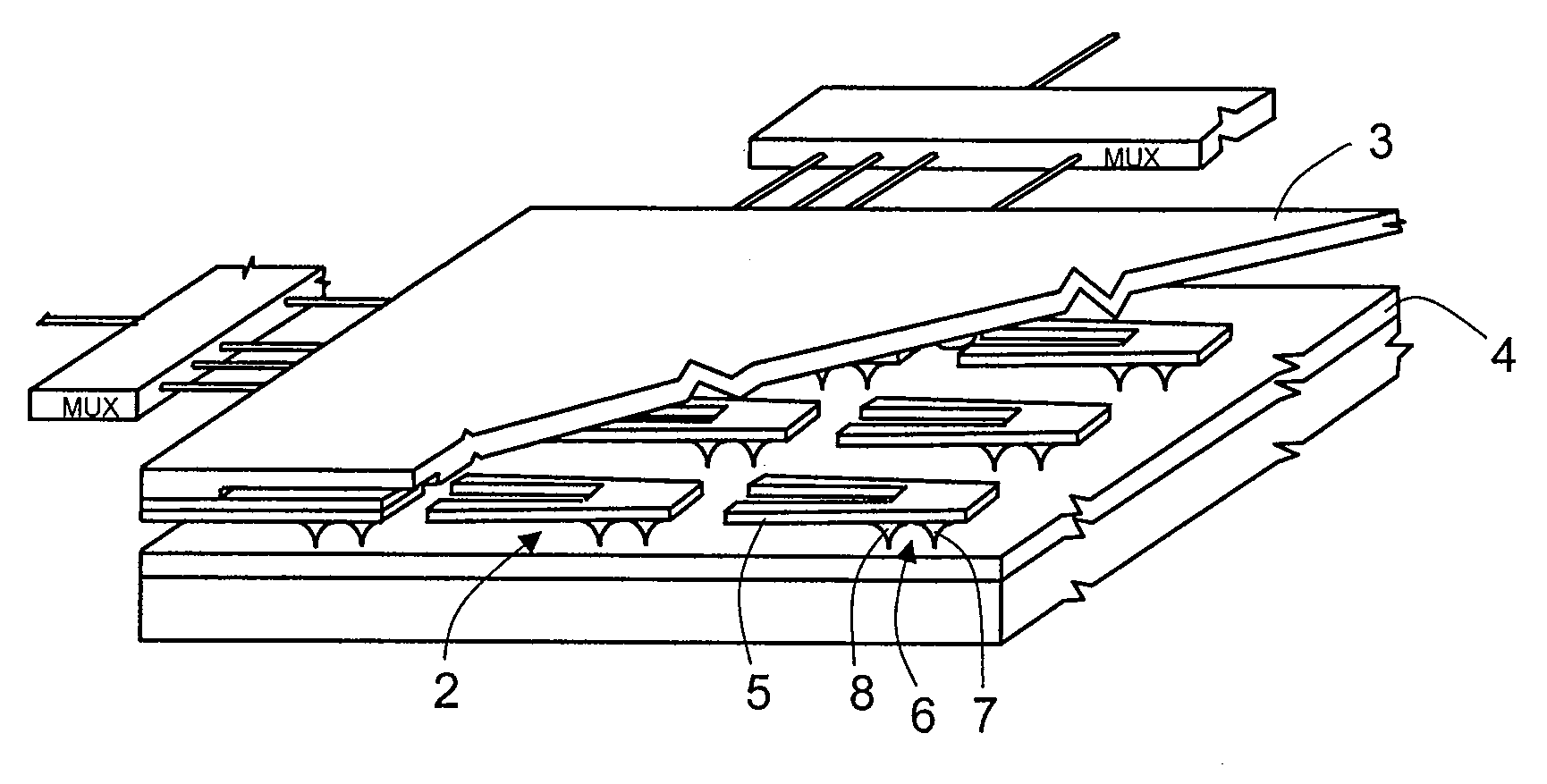
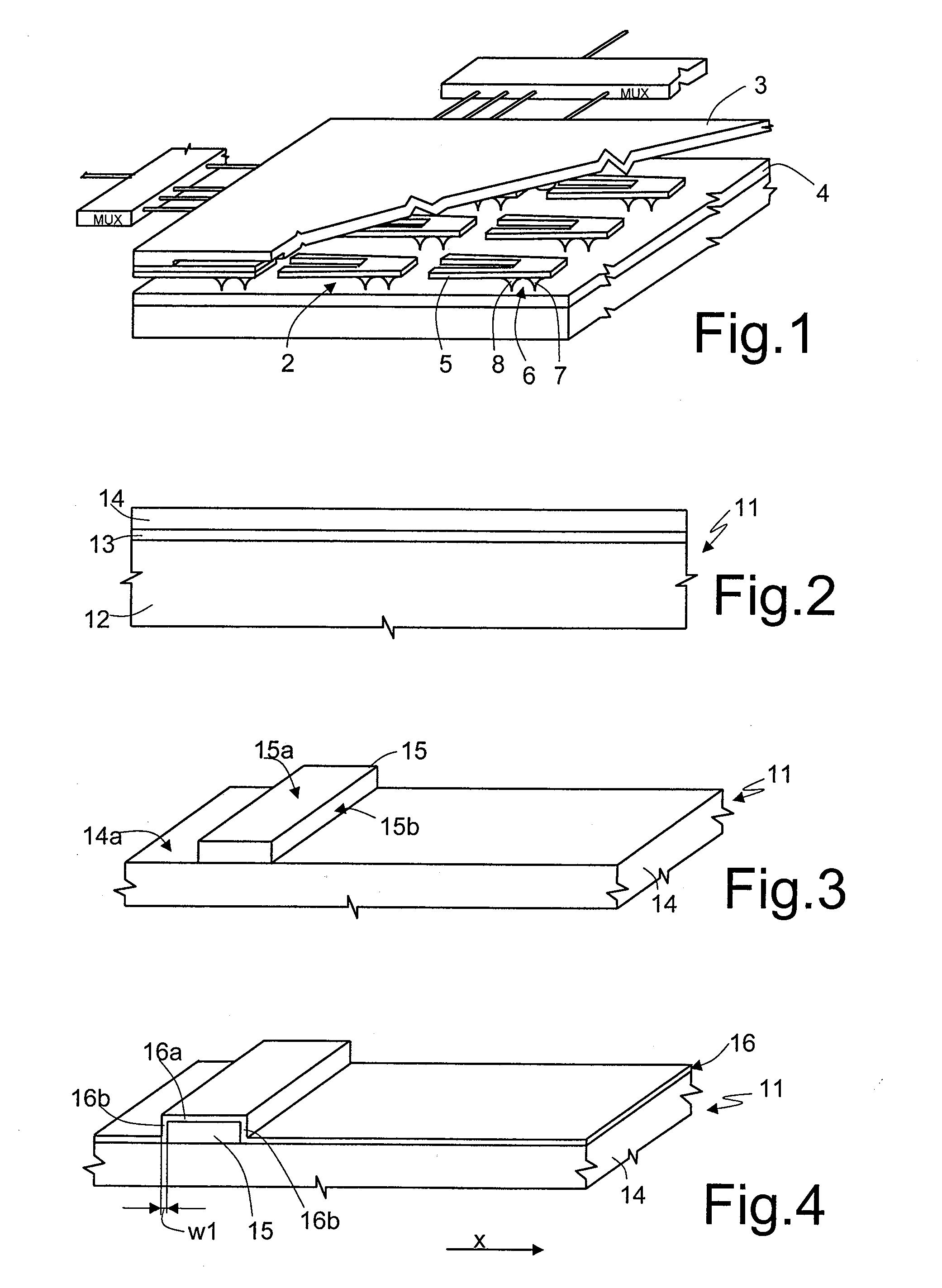
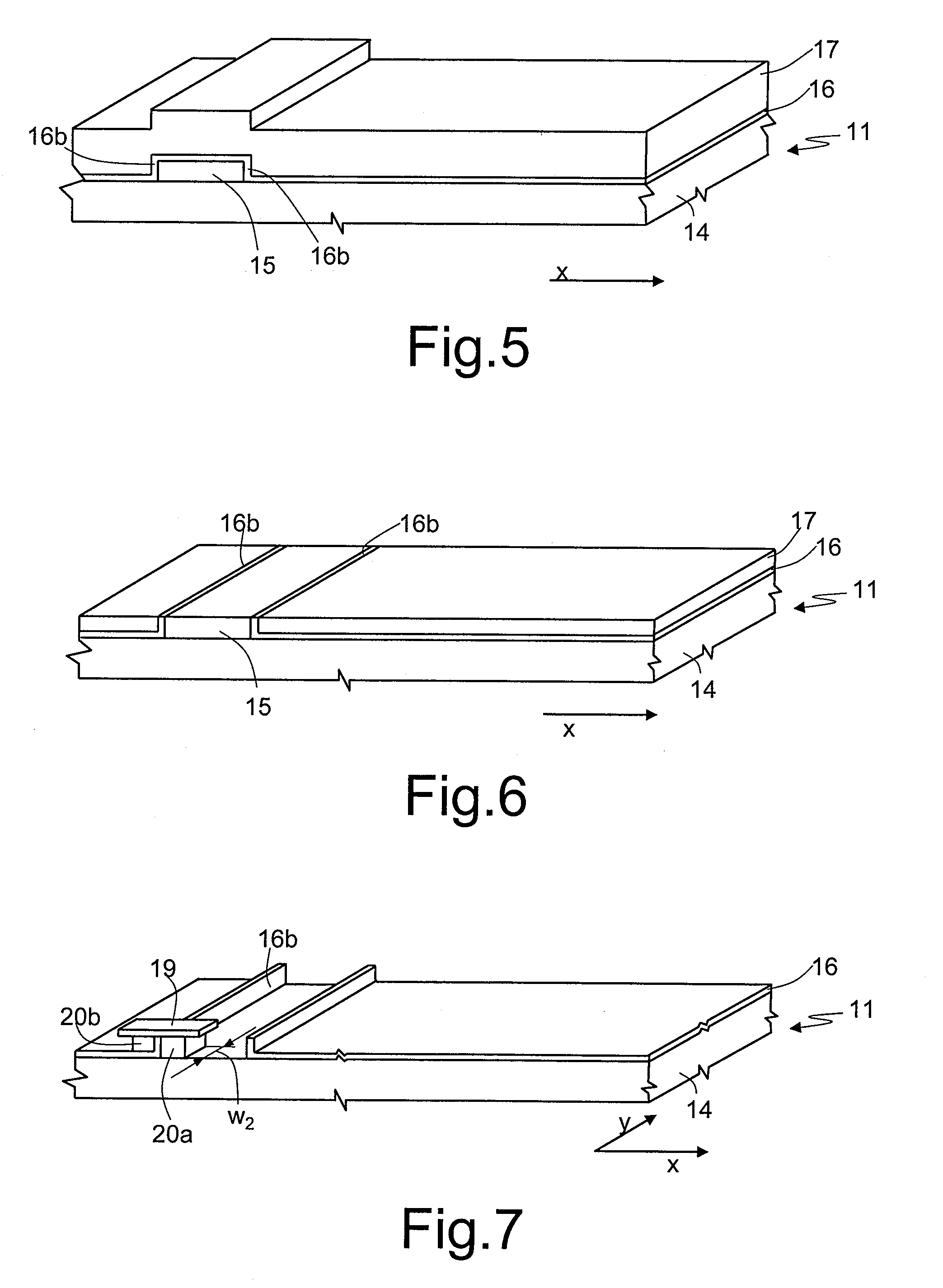
[0020]The process for manufacturing an interaction structure 6 for interaction with a storage medium 4 according to the present invention envisages (FIG. 2) formation of a wafer of semiconductor material on insulator (SOI wafer) 11, comprising a substrate 12 (which is not shown in the subsequent figures), for example made of silicon, a buried-oxide layer 13 (which is not shown in the subsequent figures either), and an epitaxial layer 14, for example made of silicon. In particular, in a per-se known manner, within the epitaxial layer 14 a supporting element 5 for the interaction structure 6 will be formed, and the thicknesses of the epitaxial layer 14 and of the buried-oxide layer 13 are consequently chosen according to the mechanical and electrical specifications that the supporting element must meet (in terms of resistivity, stiffness, etc.). For example, the epitaxial layer 14 has a thickness of 2-10 μm, and the buried-oxide layer 13 has a thickness of 0.5-2 μm.

[0021]Next, a first...

second embodiment

[0031]the present invention envisages exploitation of the process steps previously described for formation of a second interaction head 8, simultaneously to the formation of the first interaction head 7. In particular, in the case where the storage medium 4 comprises ferroelectric material, the first interaction head 7 can be a read head, whilst the second interaction head 8 can be a write head, which enables re-writing of data previously erased during the reading step.

[0032]The second embodiment differs from the first embodiment described in the shape of the first and second etching masks 19, 21.

[0033]In detail (FIG. 11), the first etching mask 19 comprises in this case a first area 19a, for definition of the insulating portions 20a, 20b belonging to the first interaction head 7, and a second area 19b, for definition of a third insulating portion 20c and a fourth insulating portion 20d which are to form, in a way similar to what has been described previously, the second interaction...


PUM


Abstract

A process manufactures an interaction structure for a storage medium. The process includes forming a first interaction head provided with a first conductive region having a sub-lithographic dimension. The step of forming a first interaction head includes: forming on a surface a first delimitation region having a side wall; depositing a conductive portion having a deposition thickness substantially matching the sub-lithographic dimension on the side wall; and then defining the conductive portion. The sub-lithographic dimension preferably is between 1 and 50 nm, more preferably 20 nm.

Description

CROSS-REFERENCE TO RELATED APPLICATION[0001]This application is a continuation-in-part of International Patent Application No. PCT / IT2006 / 000229, filed Apr. 6, 2006, now pending, which application is incorporated herein by reference in its entirety.BACKGROUND[0002]1. Technical Field[0003]The present invention relates to a process for manufacturing an interaction structure for a storage medium, in particular for “probe storage” applications, to which the ensuing treatment will make explicit reference without, however, this implying any loss of generality.[0004]2. Description of the Related Art[0005]As is known, storage systems using a magnetism-based technology, such as, for example, hard disks, suffer from major limitations as regards the increase in data-storage capacity, the read / write speed, and size reduction. In particular, a physical limit exists, referred to as “superparamagnetic limit”, which hinders reduction in the dimensions of the magnetic-storage domains below a critica...

Claims


Application Information

Patent Timeline
Patent Type & Authority Applications(United States)
IPC IPC(8): B44C1/22
CPCB82Y10/00G11B9/1409G11B9/14
Inventor RIVA, CATERINAMURARI, BRUNOFRATTINI, GIOVANNI
Owner STMICROELECTRONICS SRL
Why Eureka
Try Eureka