
Method of forming npn and pnp bipolar transistors in a CMOS process flow that allows the collectors of the bipolar transistors to be biased differently than the substrate material

a technology process flow, which is applied in the field of bipolar junction transistors, can solve the problems of not being able to bias the collector of the pnp transistor differently from the semiconductor material, and acting as a collector

Inactive Publication Date: 2009-05-21
NAT SEMICON CORP
View PDF5 Cites 4 Cited by
  • Summary
  • Abstract
  • Description
  • Claims
  • Application Information

AI Technical Summary

Benefits of technology

"The present invention relates to a method of forming bipolar junction transistors in a CMOS process flow that allows the collectors of the transistors to be biased differently than the substrate material. The technical effect of this invention is the ability to create transistors with different dopant concentrations in the source and drain regions, allowing for more precise control of their performance. This method also allows for the fabrication of high-voltage and low-voltage transistors in a single process flow, making it more efficient and cost-effective."

Problems solved by technology

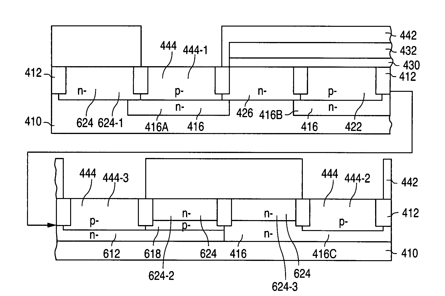
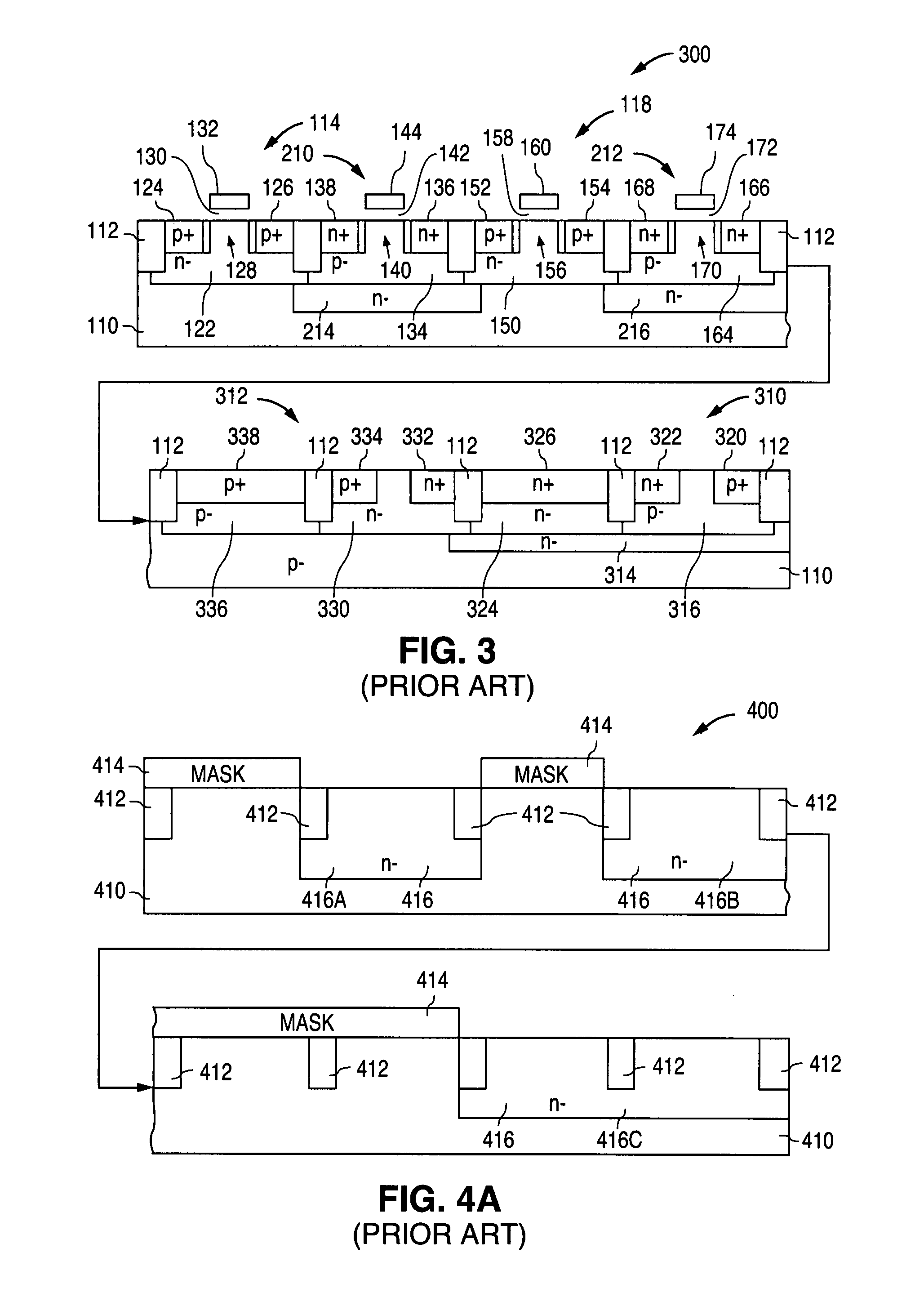
However, one of the disadvantages of the pnp transistor (e.g., transistor 312) is that semiconductor material 410 functions as part of the collector.
As a result, it is not possible to bias the collector of the pnp transistor differently from semiconductor material 410.

Method used


Image

  • Method of forming npn and pnp bipolar transistors in a CMOS process flow that allows the collectors of the bipolar transistors to be biased differently than the substrate material
  • Method of forming npn and pnp bipolar transistors in a CMOS process flow that allows the collectors of the bipolar transistors to be biased differently than the substrate material
  • Method of forming npn and pnp bipolar transistors in a CMOS process flow that allows the collectors of the bipolar transistors to be biased differently than the substrate material

Examples


Embodiment Construction

[0043]FIG. 5 shows a cross-sectional view that illustrates an example of a BiCMOS transistor structure 500 in accordance with the present invention. As described in greater detail below, BiCMOS transistor structure 500 is formed in a process that allows the collector and semiconductor material to be biased differently.

[0044]As shown in FIG. 5, BICMOS transistor structure 500 is similar to BICMOS transistor structure 300 and, as a result, utilizes the same reference numerals to designate the elements which are common to both structures. BiCMOS transistor structure 500 differs from BiCMOS transistor structure 300 in that BiCMOS transistor structure 500 utilizes a pnp transistor 512 in lieu of pnp transistor 312.

[0045]PNP transistor 512, in turn, is similar to pnp transistor 312 and, as a result, utilizes the same reference numerals to designate the structures which are common to both transistors. As further shown in FIG. 5, pnp transistor 512 differs from pnp transistor 312 in that pn...


PUM


Abstract

NPN and PNP bipolar junction transistors are formed in a semiconductor substrate material in a double polysilicon CMOS process flow in a manner that allows the collectors of both of the npn and pnp bipolar transistors to be biased differently than the bias that is placed on the semiconductor substrate material.

Description

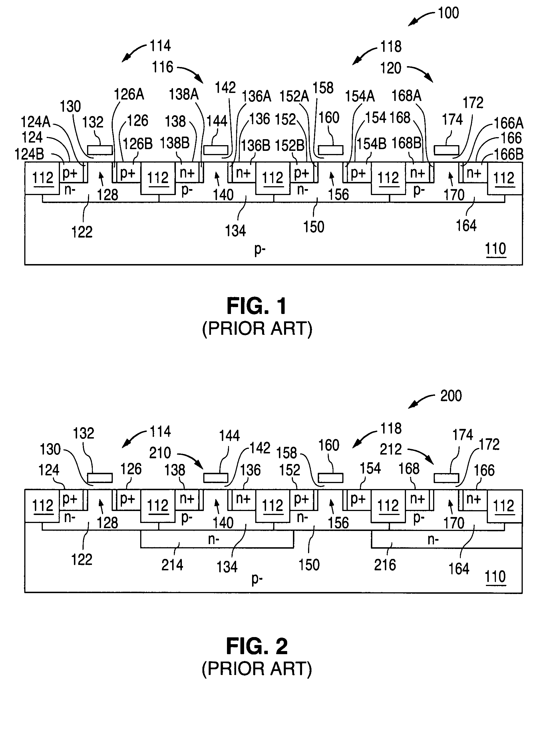
BACKGROUND OF THE INVENTION[0001]1. Field of the Invention[0002]The present invention relates to bipolar junction transistors and, more particularly, to a method of forming npn and pnp bipolar junction transistors in a CMOS process flow that allows the collectors of the bipolar transistors to be biased differently than the substrate material.[0003]2. Description of the Related Art[0004]A metal-oxide semiconductor (MOS) transistor is a well-known structure that can be fabricated as an n-channel or NMOS transistor, or as a p-channel or PMOS transistor. In addition, NMOS transistors and PMOS transistors can be fabricated as low-voltage (LV) or high-voltage (HV) transistors.[0005]FIG. 1 shows a cross-sectional view that illustrates an example of a prior-art MOS transistor structure 100. As shown in the FIG. 1 example, MOS transistor structure 100 includes a p− semiconductor material 110, such as single-crystal silicon, and a trench isolation region 112 that is formed in p− semiconductor...

Claims


Application Information

Patent Timeline
Patent Type & Authority Applications(United States)
IPC IPC(8): H01L21/8248H01L27/10
CPCH01L21/8228H01L27/082H01L27/0623H01L21/8249
Inventor SHAFI, ZIA ALAN
Owner NAT SEMICON CORP
Learn More