Methods and apparatuses for stacked capacitors for image sensors

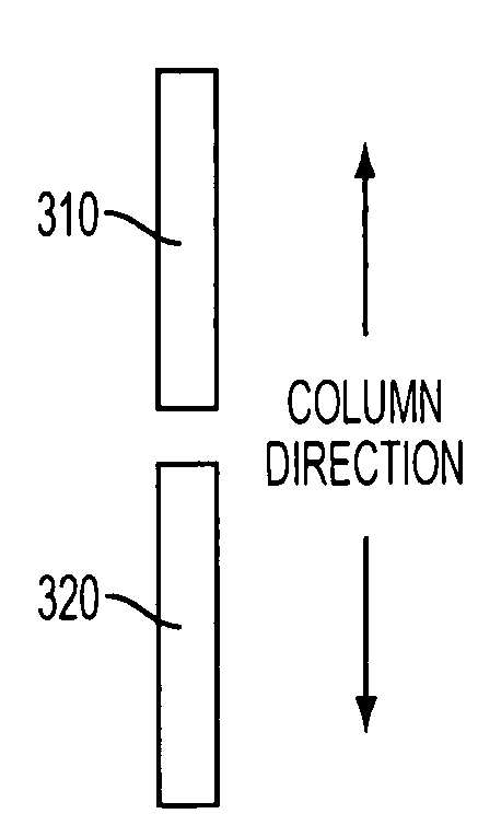
a capacitor and image sensor technology, applied in the direction of capacitors, multiple fixed capacitors, semiconductor devices, etc., can solve the problems of difficult to maintain the required capacitance within the given space, or without increasing the die size in the column direction

Inactive Publication Date: 2009-05-21
APTINA IMAGING CORP
View PDF24 Cites 69 Cited by
  • Summary
  • Abstract
  • Description
  • Claims
  • Application Information

AI Technical Summary

Problems solved by technology

As the column pitch of the array becomes smaller to support higher density resolutions, the space available for the sample and hold capacitors becomes constrained, and it becomes difficult to maintain the required capacitance within the given space, or without increasing die size in the column direction.

Method used


Image

  • Methods and apparatuses for stacked capacitors for image sensors
  • Methods and apparatuses for stacked capacitors for image sensors
  • Methods and apparatuses for stacked capacitors for image sensors

Examples


Embodiment Construction

[0027]In the following detailed description, reference is made to the accompanying drawings, which form a part hereof and show by way of illustration specific embodiments in which embodiments of the present invention may be practiced. These embodiments are described in sufficient detail to enable those skilled in the art to practice them, and it is to be understood that other embodiments may be utilized, and that structural, logical, processing, and electrical changes may be made. The progression of processing steps described is an example; however, the sequence of steps is not limited to that set forth herein and may be changed as is known in the art, with the exception of steps necessarily occurring in a certain order.

[0028]Now referring to the figures, where like numerals designate like elements, FIG. 4A is a circuit diagram of a capacitive circuit including a multi-layer sample and hold capacitor 400 constructed in accordance with an embodiment described herein. The multi-layer ...


PUM


Abstract

Capacitive circuits and methods of forming capacitive circuits including a first capacitor and a second capacitor connected in parallel to the first capacitor, wherein the first capacitor is positioned at least partially above the second capacitor.

Description

FIELD OF THE INVENTION[0001]Disclosed embodiments relate generally to the field of image sensors employing capacitors.BACKGROUND OF THE INVENTION[0002]The constant drive for higher resolution, higher pixel density image sensors has pushed the pixel size, and thus the row / column pitch, of the pixel array to the point where column readout circuitry is being constrained to fit within the required pitch.[0003]FIG. 1 illustrates, in a simplified block diagram, an imaging device 100 having a CMOS pixel array 140. Row lines of the array 140 are selectively activated by a row driver 145 in response to row address decoder 155. A column driver 160 and column address decoder 170 are also included in the imaging device 100. The imaging device 100 is operated by the timing and control circuit 150, which controls the address decoders 155, 170. The control circuit 150 also controls the row and column driver circuitry 145, 160.[0004]A sample and hold circuit 200 associated with the column driver 16...

Claims


Application Information

Patent Timeline
Patent Type & Authority Applications(United States)
IPC IPC(8): H01G4/38H01L21/20
CPCH01G4/30H01L27/14609H01L27/0805H01G4/38
Inventor MAURITZSON, RICHARD A.
Owner APTINA IMAGING CORP
Why Eureka
Try Eureka