

Device mounting board and manufacturing method therefor, and semiconductor module
a technology of semiconductor modules and mounting boards, which is applied in the direction of solid-state devices, electrical apparatus construction details, basic electric elements, etc., can solve the problems of reducing the restrictive factors of the narrowing of the pitch of the electrode, and the drop of the reliability of connection between the semiconductor device and the printed wiring board
- Summary
- Abstract
- Description
- Claims
- Application Information
AI Technical Summary
Benefits of technology
Problems solved by technology
Method used
Image

Examples
first embodiment
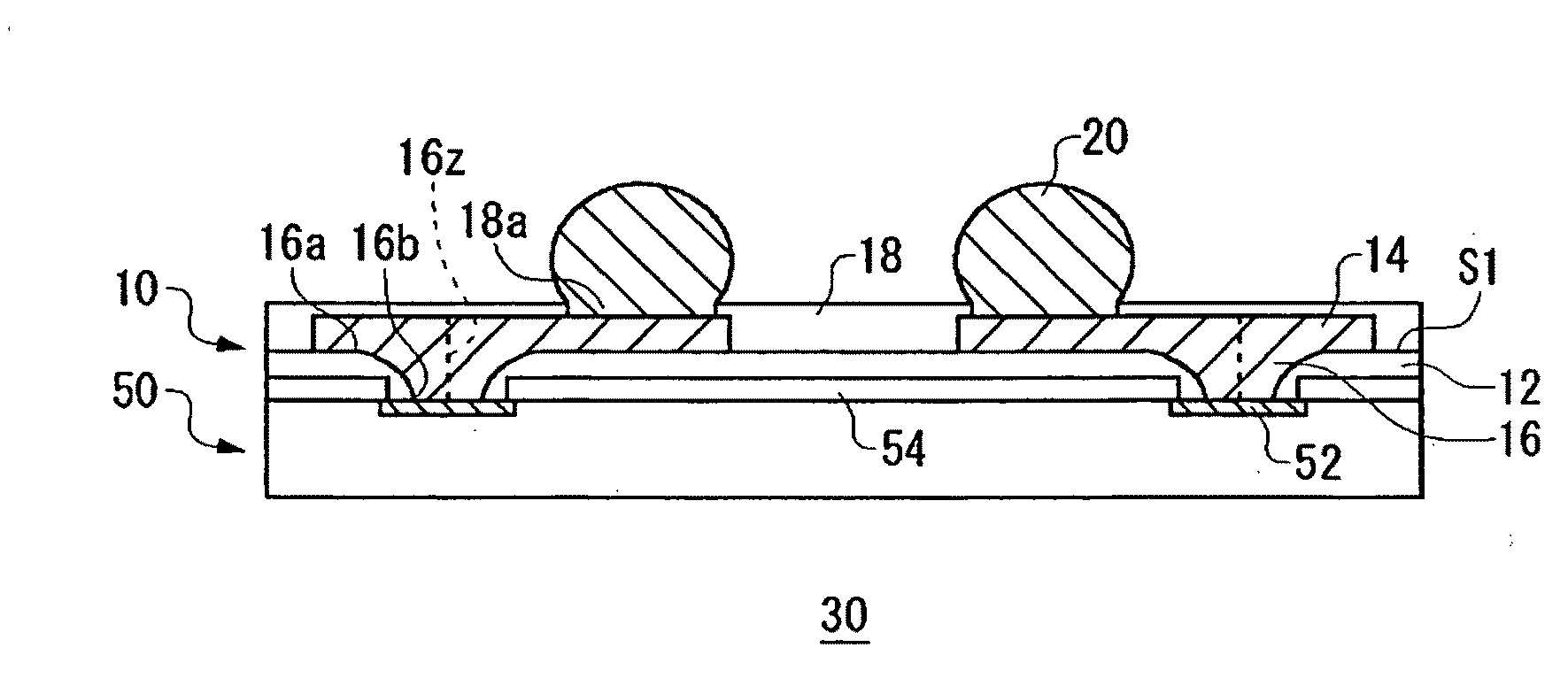
[0044]FIG. 1 is a schematic cross-sectional view illustrating a structure of a device mounting board 10 according to a first embodiment of the present invention and a structure of a semiconductor module 30 using said device mounting board 10. The semiconductor module 30 includes a device mounting board 10 and a semiconductor device 50 mounted on the device mounting board 10.
[0045]The device mounting board 10 includes an insulating resin layer 12, a wiring layer 14 provided on one main surface S1 of the insulating resin layer 12, and a bump electrode 16, connected electrically to the wiring layer 14, which protrudes on a side of the insulating resin layer 12 from the wiring layer 14.
[0046]The insulating resin layer 12 is made of insulating resin and is formed of, for example, a material that develops plastic flow when pressurized. An example of the material that develops plastic flow when pressurized is epoxy thermosetting resin. The epoxy thermosetting resin to be used for the insul...
second embodiment
[0073]As a result of careful investigation, the inventors have realized that thermal stress can be concentrated more in the side surface of the bump electrode on the side to which the wiring layer extends than in the side surface thereof on the opposite side. They have also found that when the insulating resin layer is approximately square in shape in a plan view, thermal stress tends to be concentrated in the side surface, on the side to which the wiring layer extends, of the bump electrode located close to corners (edges) of the insulating resin layer. And the second embodiment had been conceived by the inventors based on these realizations.
[0074]FIG. 6 is a schematic cross-sectional view illustrating a structure of a device mounting board 1010 having a bump structure according to a second embodiment of the present invention and a structure of a semiconductor module 1030 using said device mounting board 1010. The semiconductor module 1030 includes a device mounting board 1010 and ...
third embodiment
[0111]FIG. 14 is a schematic cross-sectional view showing a structure of a device mounting board 2010 having a bump structure according to a third embodiment of the present invention and a structure of a semiconductor module 2030 using said device mounting board 2010. The semiconductor module 2030 includes a device mounting board 2010 and a semiconductor device 2050 mounted on the device mounting board 2010.
[0112]The device mounting board 2010 includes an insulating resin layer 2012, a wiring layer 2014 provided on one main surface S2001 of the insulating resin layer 2012, and a bump electrode 2016, connected electrically to the wiring layer 2014, which protrudes on a side of the insulating resin layer 2012 from the wiring layer 2014.
[0113]The insulating resin layer 2012 is made of insulating resin and is formed of, for example, a material that develops plastic flow when pressurized. An example of the material that develops plastic flow when pressurized is epoxy thermosetting resin....
PUM
 Abstract
Description
Claims
Application Information