Image pickup device and signal processing method thereof

a pickup device and image technology, applied in the field of image pickup devices and signal processing methods thereof, can solve the problems of increasing the number/volume of wirings, reducing the conversion speed to 12, and fatal to digital camera applications requiring high-speed shutter and moving image applications

Inactive Publication Date: 2009-10-01
CANON KK
View PDF12 Cites 73 Cited by
  • Summary
  • Abstract
  • Description
  • Claims
  • Application Information

AI Technical Summary

Problems solved by technology

However, correction according to a method being discussed in Japanese Patent Application Laid-Open No. 2006-025189 has the following three problems: The first is that analog-to-digital conversion is always required twice, which causes, in principle, a conversion speed to be lowered to ½. This problem is fatal to digital camera application requiring high-speed shutter and moving image application.
A column ADC must be laid out in almost the same width or at a maximum several times as wide as pixels of the image sensor and an increase in the number / volume of wirings, capacitance or switches will impair pixel size reduction or cause characteristic degradation.
However, if conversion result as indicated by 1611 is obtained in place of 1610 by external disturbance due to random noise of pixels or a read-out circuit or the like, averaging will not make the obtained result meet the ideal characteristic, resulting in a correction error.
The lookup table varies with individual analog-to-digital converters, which makes it difficult to realize commonality for a plurality of analog-to-digital converters.
Accordingly, as the number of the analog-to-digital converters increases, such a sensor is difficult to apply for practical use.
In particular, where a pixel region arranged with a plurality of pixels including photoelectric transfer elements and a reading unit including analog-to-digital converters are disposed on an identical semiconductor substrate, restriction on layout of elements is strict and, in some cases, an extreme increase in circuit scale causes a particular problem due to the increased number of correction circuits.

Method used


Image

  • Image pickup device and signal processing method thereof
  • Image pickup device and signal processing method thereof
  • Image pickup device and signal processing method thereof

Examples


first embodiment

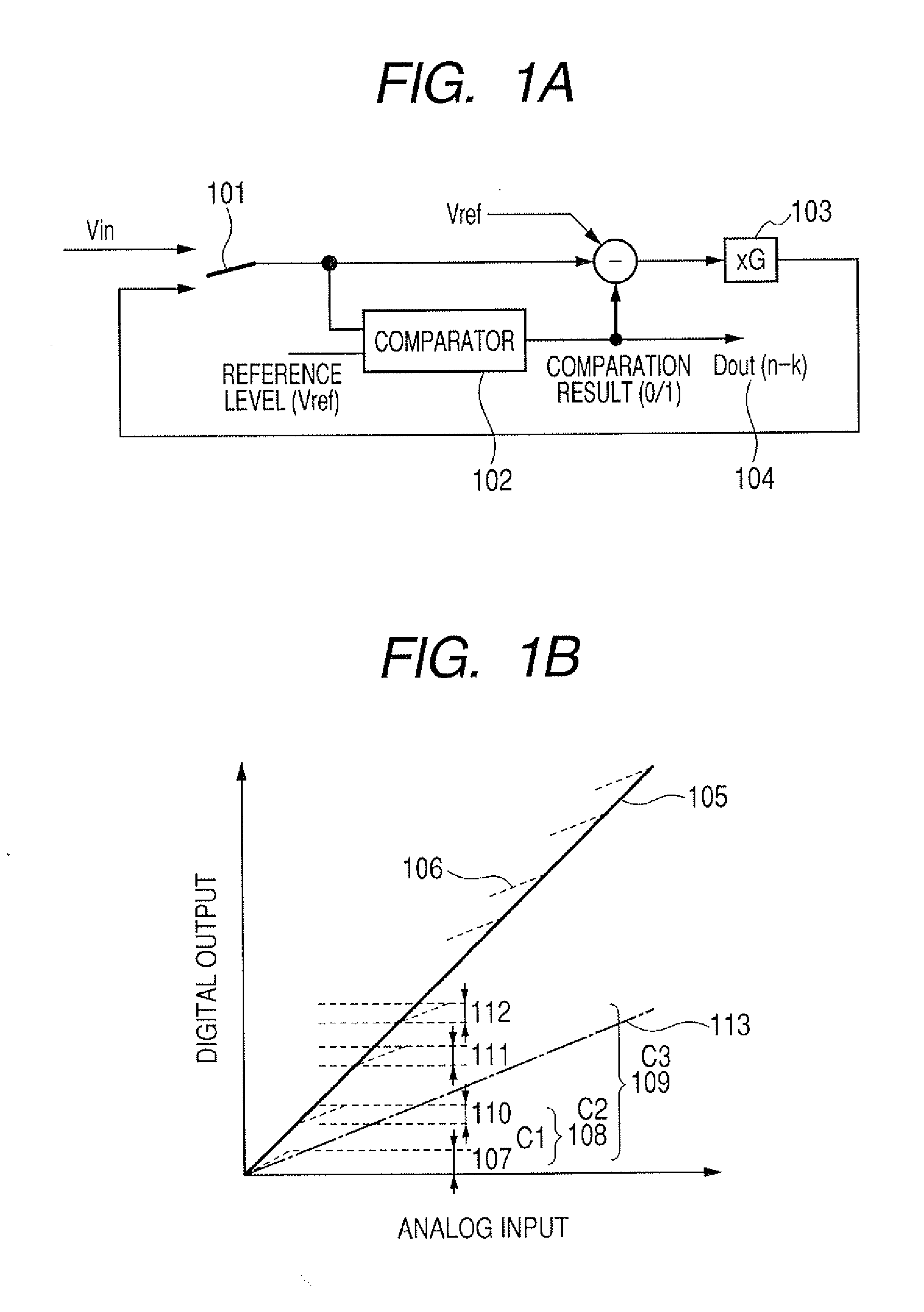
[0036]FIGS. 1A, 1B and 2 are a view illustrating an analog-to-digital converter according to a first embodiment of the present invention, respectively. FIG. 1A is a circuit block diagram illustrating a configurational example of a circulation type of an analog-to-digital converter (ADC) used for a column ADC. FIG. 1B illustrates an example of I / O characteristics of ADC with digital outputs Dout corresponding to analog inputs Vin plotted. I / O characteristics are illustrated by a continuous line for description. 3-bit is estimated herein, and it is assumed that a digital value of 3-bit precision quantized for a specific analog value is obtained. It is actually rare that correction is necessary for 3-bit AD conversion, which is a assumption for simplifying a drawing, so as to make a simplified description.

[0037]A signal Vin from a pixel input into an input terminal 101 is compared with a reference level Vref by a comparator 102 and the comparison result becomes a digital code. When the...

second embodiment

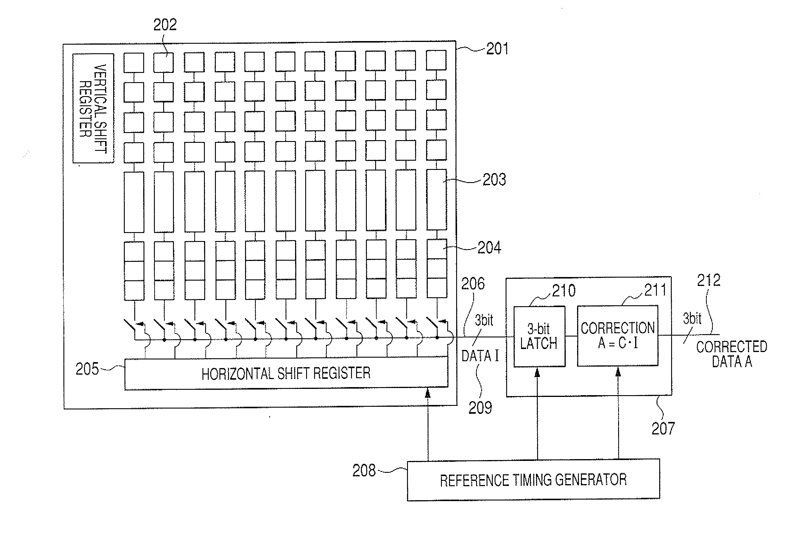
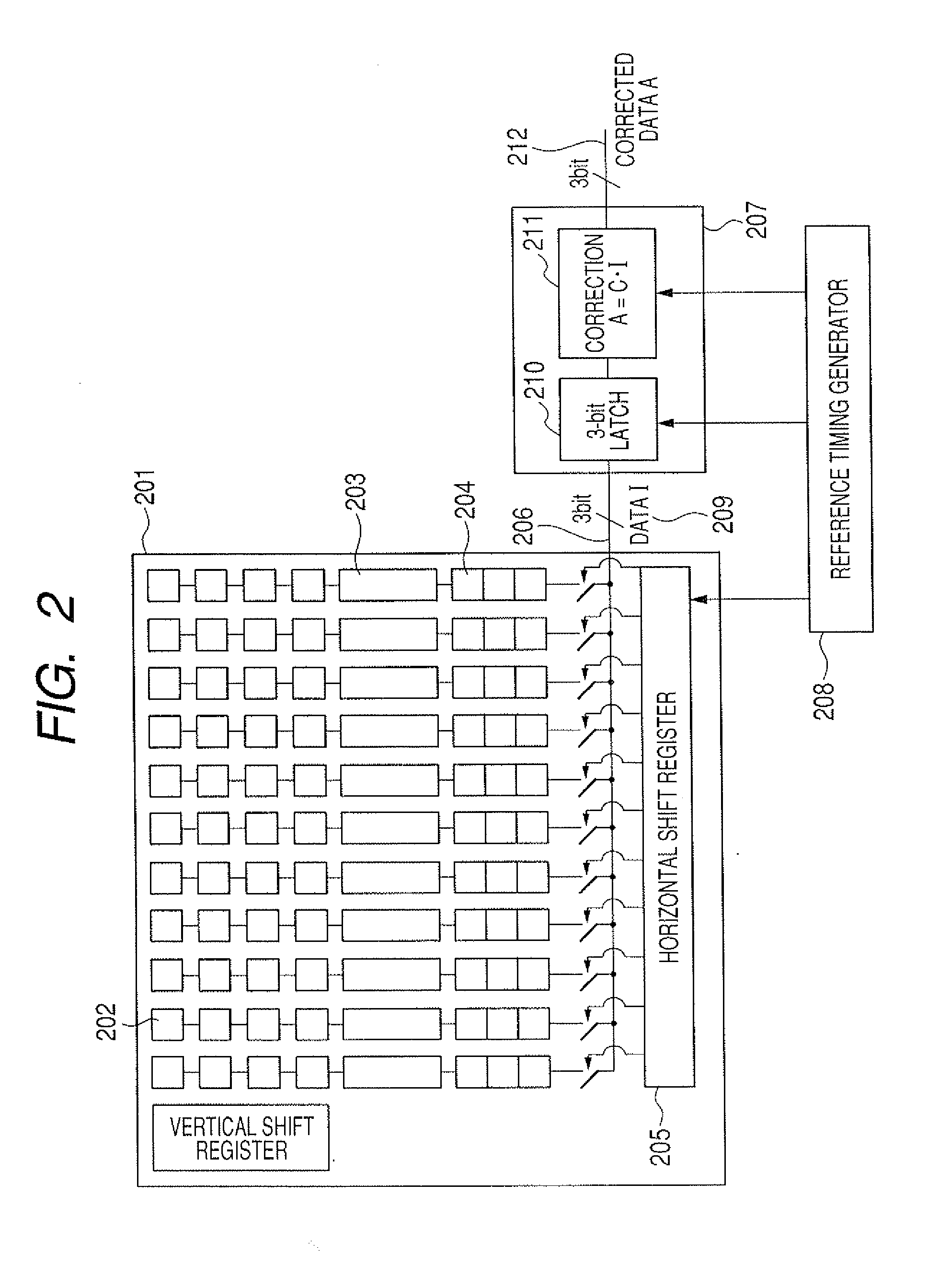
[0055]As described above, the column ADC is laid out in the same width or at a maximum several times as wide as the pixel. This makes it difficult to ensure local precision of an analog element. Variations in the local precision at each column causes variations in gain of the amplifier 103 according to a first embodiment at each column, and use of the same correction factor would not ensure precision after correction. Accordingly, it is necessary to prepare correction factors for each column and perform correction with unique correction factors for each column ADC.

[0056]FIG. 3 shows a configurational example of the image pickup device having a column ADC according to a second embodiment of the present invention for solving the foregoing problems, and has the same reference numerals for the same portions as those in FIG. 2. A different point from those in the first embodiment is an added correction factor memory 301, and the memory 301 operates with a control signal 302 input from th...

third embodiment

[0063]In a third embodiment according to the present invention, a correction factor acquirement unit for acquiring the correction factor from an actual CMOS image sensor will be described below. FIGS. 5A to 5C illustrates I / O characteristics of an analog-to-digital converter to be corrected according to this embodiment. FIG. 6 illustrates a configurational example of a column ADC capable of obtaining a correction factor according to this embodiment. The same portions as those in FIGS. 1A and 1B have the same numerals.

[0064]FIG. 5A illustrates an example when an erroneous code occurs just in the center of an input dynamic range. The following is a method for determining one element Cn of the correction factor as indicated by reference numeral 501. FIG. 6 illustrates an example of a correctable column ADC circuit capable of determining Cn.

[0065]First, an input is provided with a path for inputting signals 601, 602, 603 from a column and a path for circulating signals themselves, as we...


PUM


Abstract

An image pickup device is provided, capable of complete correction with data of once analog-to-digital conversion, and prevention of excess use of switches and analog devices and / or erroneous correction, including: an image sensor having a plurality of analog-to-digital converters determining conversion results from a digital signal of higher order bit through separate steps of two or more times; a first correction unit which has a correction factor for correcting nonlinear errors of the plurality of analog-to-digital converters so as to adapt to the analog-to-digital converters and corrects a nonlinear error of a digital signal output from respective analog-to-digital converters based on a correction factor corresponding to respective analog-to-digital converters, characterized in that the first correction unit corrects the nonlinear errors after converting the digital signals from the plurality of analog-to-digital converters into a serial output.

Description

TECHNICAL FIELD[0001]The present invention relates to an image pickup device and a signal processing method thereof.BACKGROUND ART[0002]Some CMOS image sensors have analog-to-digital converters in parallel to each other in a column to read signals from the sensors at a high speed. Such analog-to-digital converters arranged in parallel in a column are referred to as a “column ADC”.[0003]FIG. 15 is a schematic diagram of I / O characteristics of an analog-to-digital converter. Where the precision of an analog circuit is as ideal during amplification, a straight line is shown as indicated by 1501. In the case where a deviation is made from the ideal line as indicated by dashed lines 1502, a digital code (an erroneous code) which will not appear even if any analog data is input occurs.[0004]As an example of a prior art against the problem, Japanese Patent Application Laid-Open No. 2006-025189 discusses an image sensor that has a circulation type of analog-to-digital converter for each col...

Claims


Application Information

Patent Timeline
Patent Type & Authority Applications(United States)
IPC IPC(8): H04N5/217H03M1/06H04N5/335H04N5/341H04N5/361H04N5/365H04N5/369H04N5/374H04N5/378
CPCH04N5/357H04N5/3745H04N5/378H04N25/60H04N25/75H04N25/77
Inventor YAMASHITA, YUICHIRO
Owner CANON KK
Why Eureka
Try Eureka