Partially underfilled solder grid arrays

a solder grid and array technology, applied in the direction of printed circuit aspects, sustainable manufacturing/processing, final product manufacturing, etc., can solve the problems of mechanically weak interconnections, lead-free interconnections can become damaged and even fall off, and the rework is difficul

Inactive Publication Date: 2009-10-15
GLOBALFOUNDRIES INC
View PDF6 Cites 10 Cited by
  • Summary
  • Abstract
  • Description
  • Claims
  • Application Information

AI Technical Summary

Problems solved by technology

One is that the strength of low-lead and lead-free interconnect is significantly less than that of high-lead interconnects resulting in mechanically weak interconnections.
A second is low-l

Method used


Image

  • Partially underfilled solder grid arrays
  • Partially underfilled solder grid arrays
  • Partially underfilled solder grid arrays

Examples


Embodiment Construction

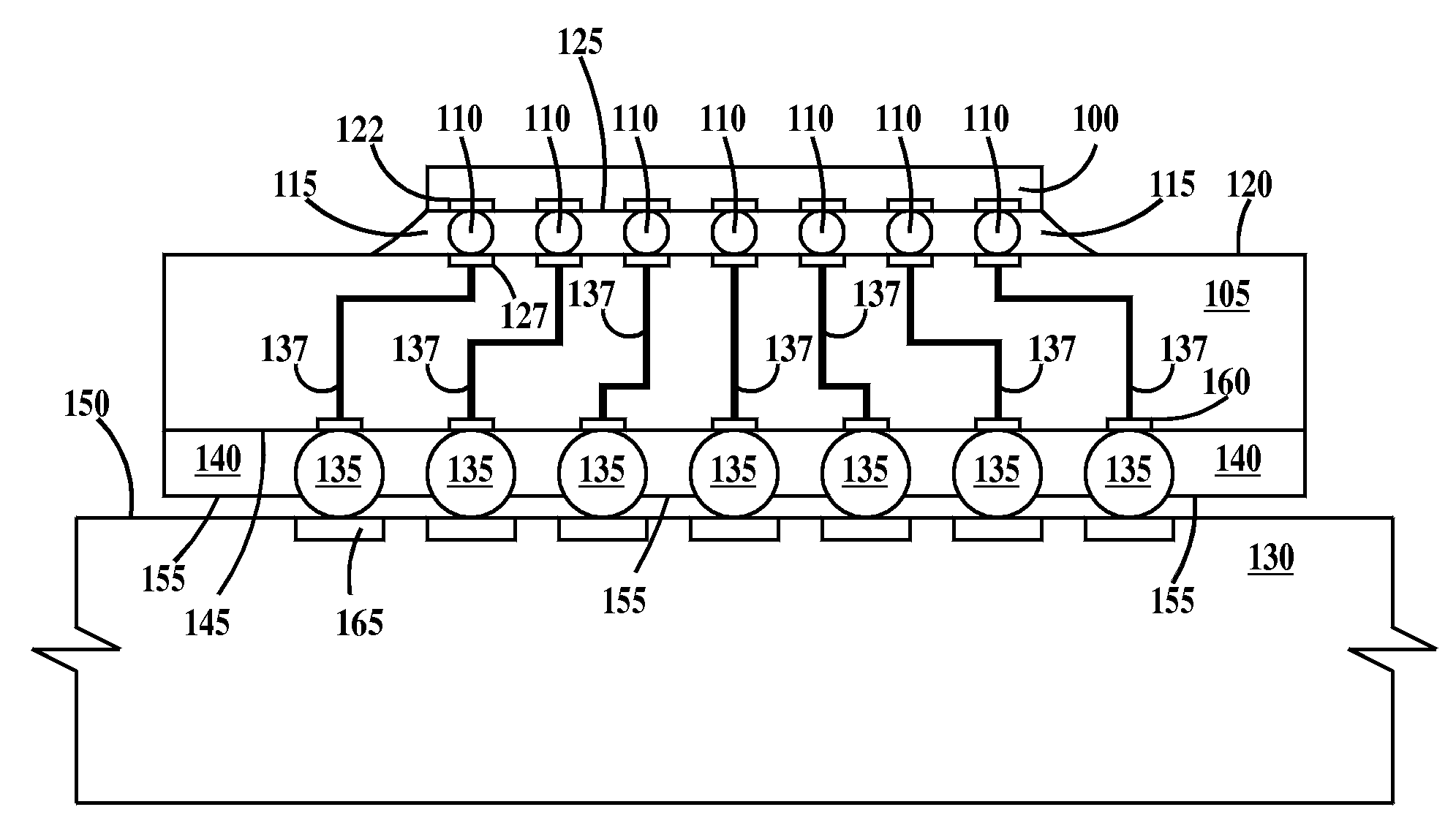
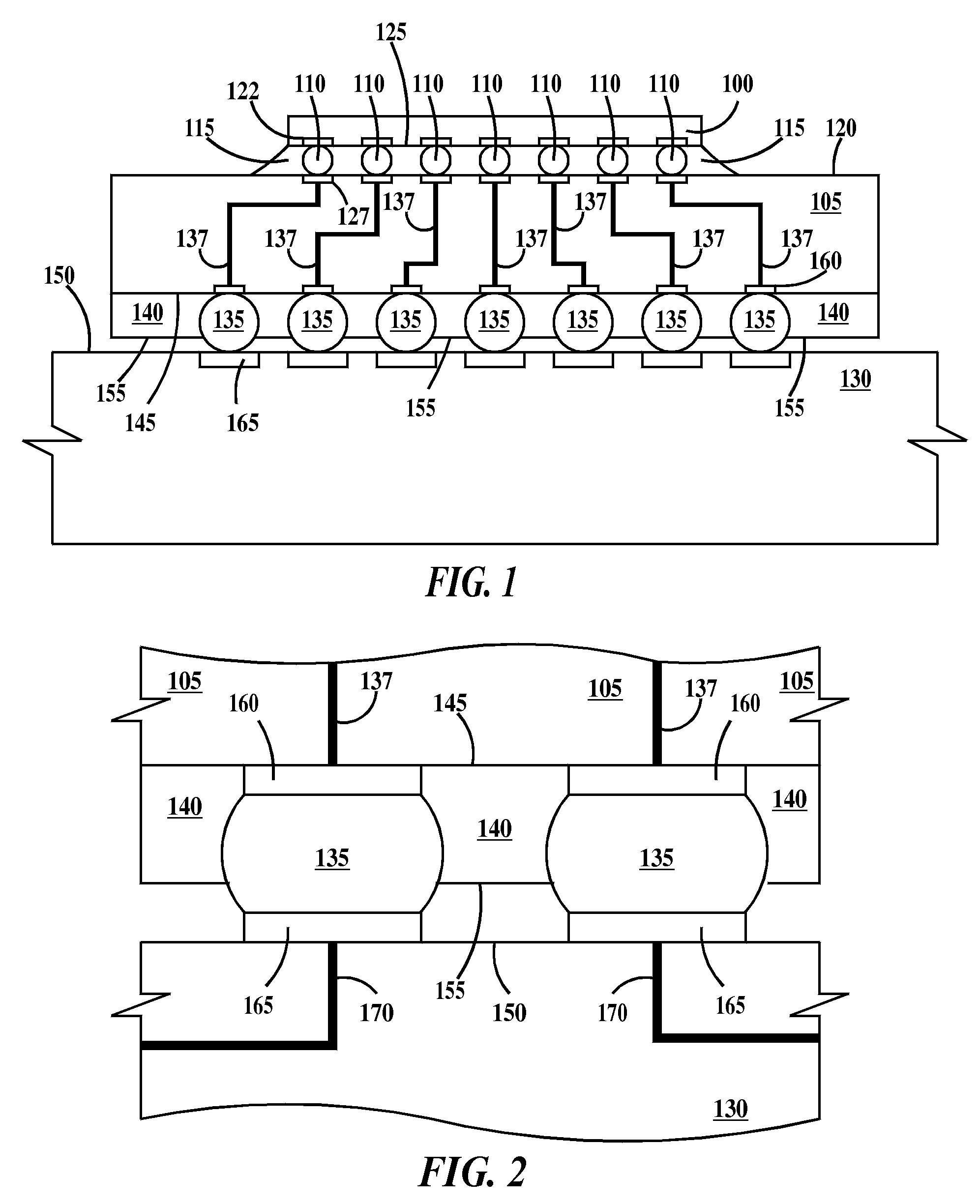
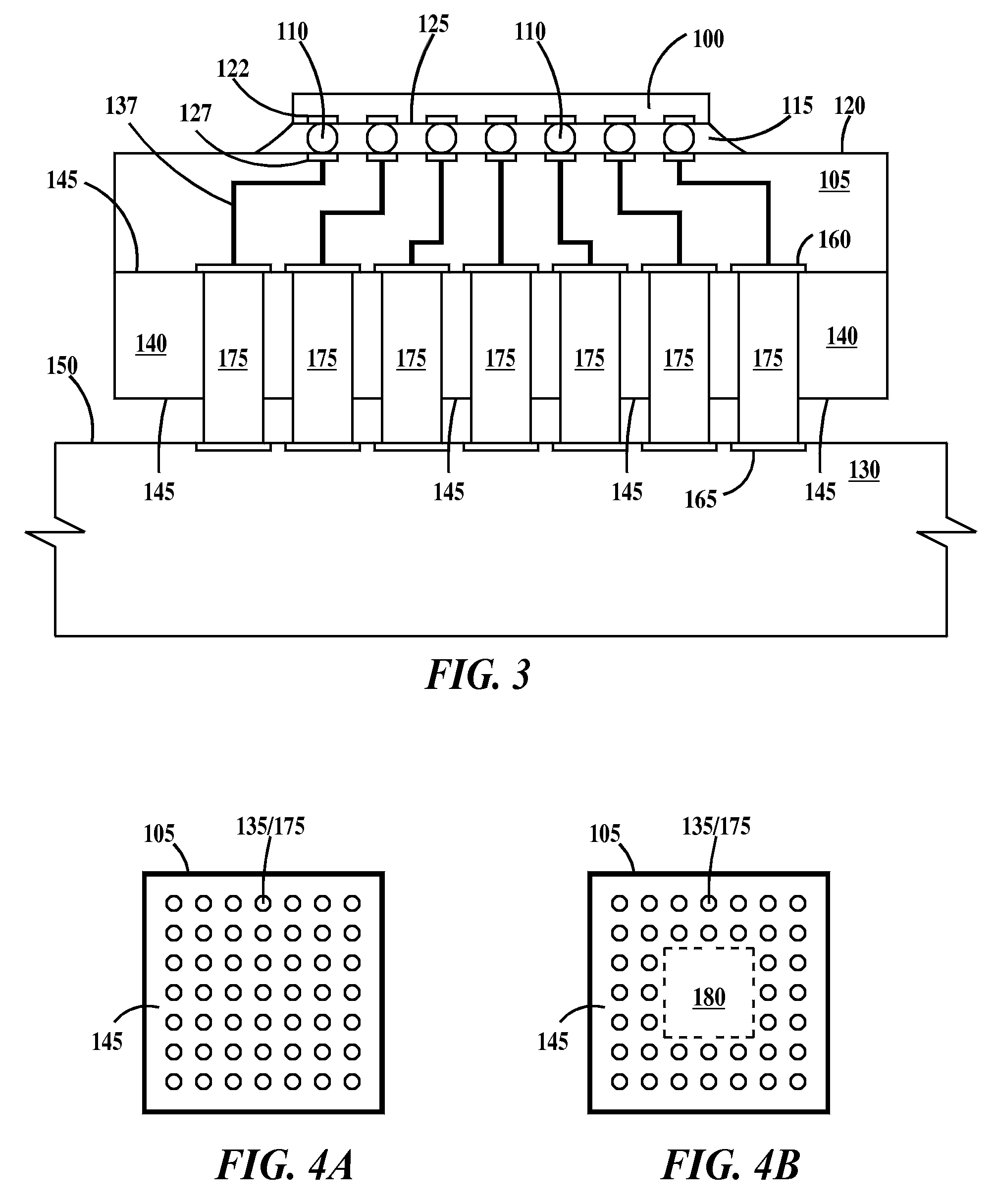
[0011]An integrated circuit module is first level packaging element intermediate between an integrated circuit chip and second level packaging element, examples of second level packages include but are not limited to a printed circuit boards and printed circuit cards. A printed circuit board includes one or more wiring levels embedded in and / or on one or more surfaces of an organic based dielectric material (which may include non-organic materials like fiberglass). Integrated circuit modules are physically mounted and electrically connected to printed circuit boards by metallurgical interconnects. Examples of module types include ceramic modules (wires on or embedded in a ceramic substrate), multilayer ceramic modules (multiple levels of wires on and / or embedded in multiple layers of ceramic material) and printed circuit boards. A lead-free interconnect is defined as metallurgical interconnect containing none to less than about 0.01% lead. A low lead interconnect is defined as a met...


PUM


Abstract

An electronic device and a method of forming the device. The device including a module having opposite top surface and bottom surfaces; a first set of pads on the top surface of the module and a second set of pads on the bottom surface of the module substrate, wires within the module electrically connecting the first set of pads to the second set of pads; a set of solder interconnects in electrical and physical contact with a the second set of module pads; and a dielectric underfill layer formed on the bottom surface of the module, the underfill layer filling the space between lower regions of the solder interconnects of the set of solder interconnects, upper regions of the solder interconnects of the set of solder interconnects extending past a top surface of the underfill layer.

Description

FIELD OF THE INVENTION[0001]The present invention relates to the field of integrated circuit packaging; more specifically, it relates to structures and methods of mounting integrated circuit modules to circuit boards.BACKGROUND OF THE INVENTION[0002]The industry trend to move from lead containing interconnects between integrated circuit modules and printed circuit boards and cards to low-lead and lead-free interconnects has introduced some unique challenges. One is that the strength of low-lead and lead-free interconnect is significantly less than that of high-lead interconnects resulting in mechanically weak interconnections. A second is low-lead and lead-free interconnects can become damaged and even fall off prior to card attachment. A third is rework is difficult as some interconnects may be lost during the dis-attach process.[0003]Accordingly, there exists a need in the art to overcome the deficiencies and limitations described hereinabove.SUMMARY OF THE INVENTION[0004]A first ...

Claims


Application Information

Patent Timeline
IPC IPC(8): H01L23/48
CPCH01L23/49816H01L23/49827H01L2224/32225H05K2203/0415H05K2201/10977H05K2201/10734H05K3/3436H01L2924/15311H01L2924/14H01L2224/73204H01L24/16H01L2224/16225H01L2924/00H01L2224/05571H01L2224/05573H01L2924/00014Y02P70/50H01L2224/05599
Inventor AYOTTE, STEPHEN PETERPEPI, CHRISTINA MARIESULLIVAN, TIMOTHY M.
Owner GLOBALFOUNDRIES INC
Why Eureka
Try Eureka