Semiconductor die package including die stacked on premolded substrate including die

Inactive Publication Date: 2009-11-12
LIU YONG +2
View PDF63 Cites 19 Cited by
  • Summary
  • Abstract
  • Description
  • Claims
  • Application Information

AI Technical Summary

Problems solved by technology

Another problem to be solved is to provide for the ability to dissipate heat from a semiconductor die comprising a power transistor in a semiconductor die package including multiple dice.
For example, if a power transistor die and an integr

Method used


Image

  • Semiconductor die package including die stacked on premolded substrate including die
  • Semiconductor die package including die stacked on premolded substrate including die
  • Semiconductor die package including die stacked on premolded substrate including die

Examples


Embodiment Construction

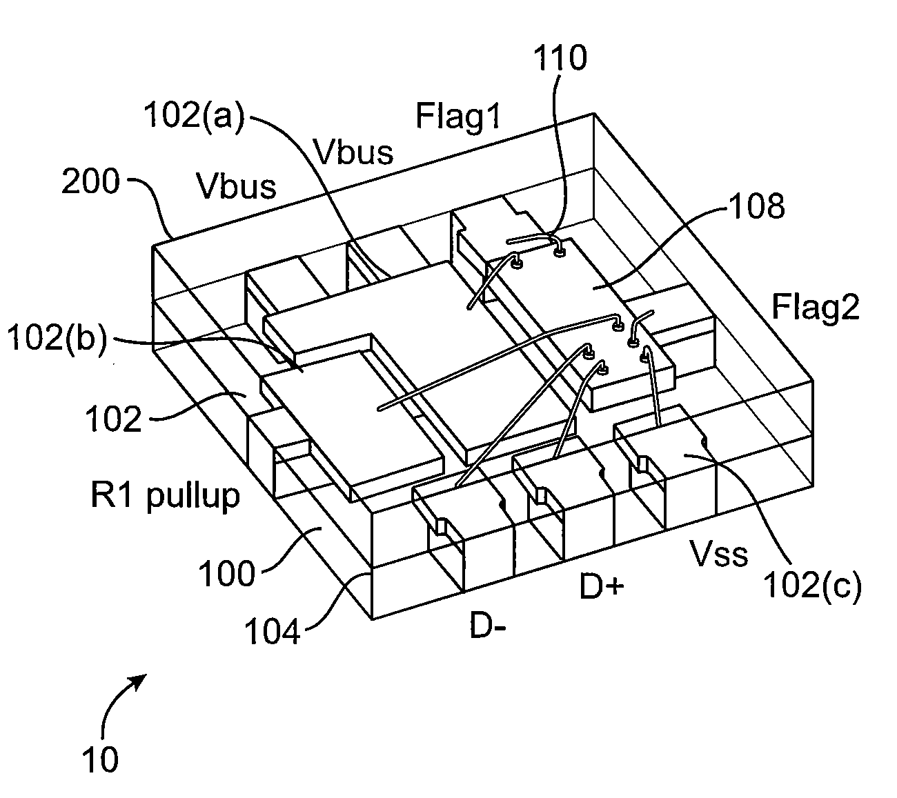
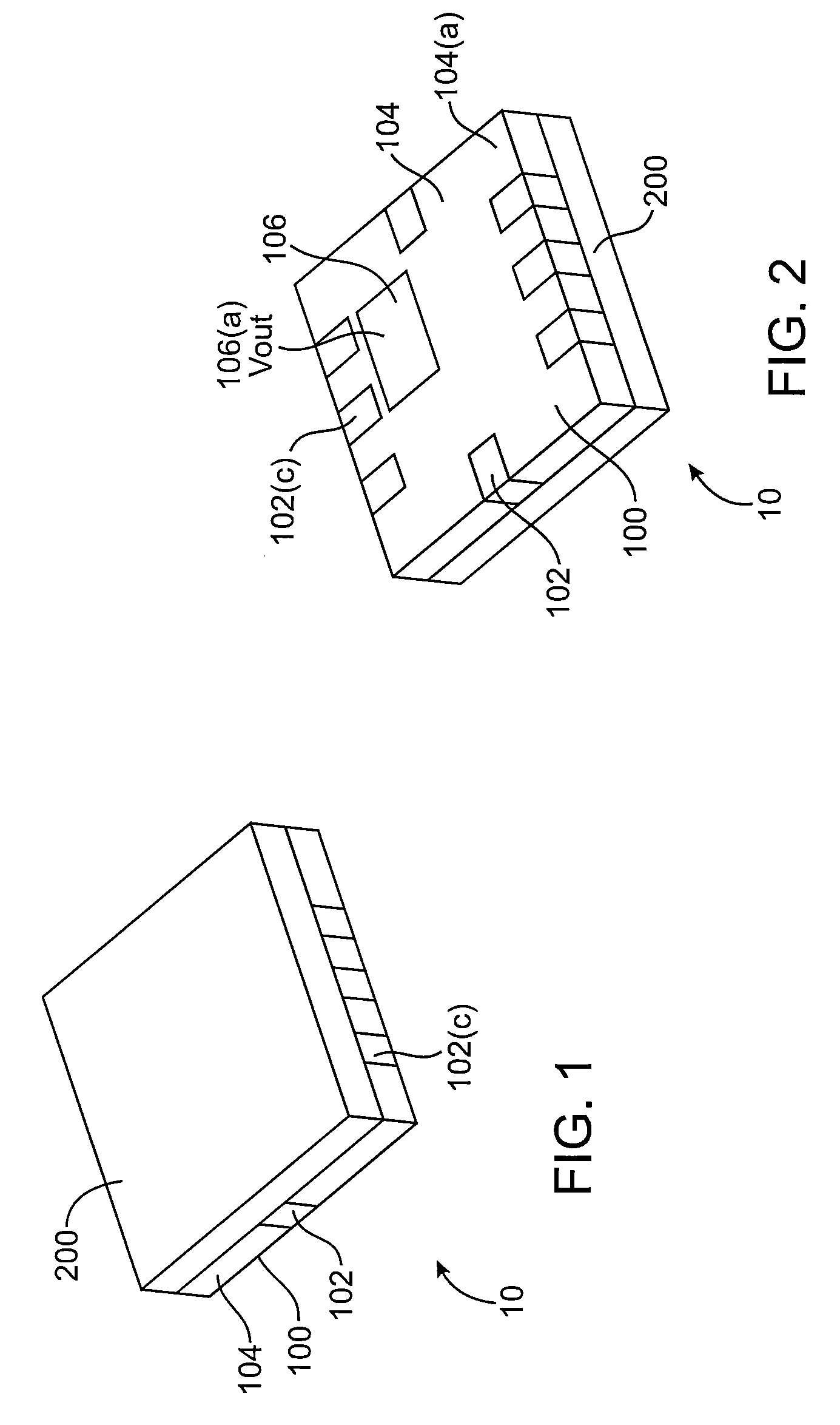
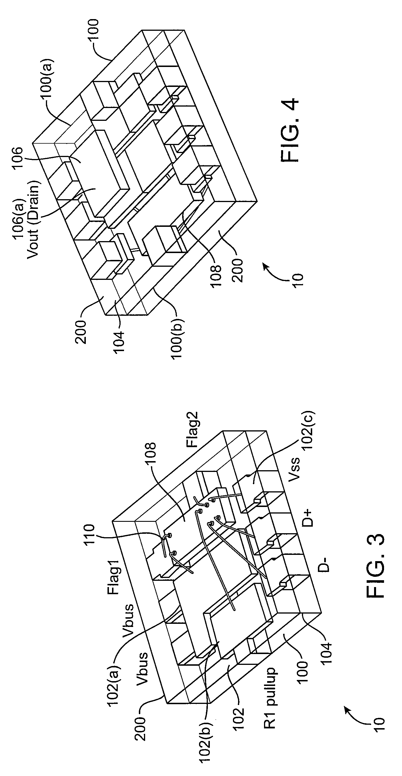
[0023]A number of embodiments of the invention are described herein. Embodiments of the invention include methods for electrically interconnecting an IC (integrated circuit) die and a MOSFET (metal oxide semiconductor field effect transistor) die through a premolded substrate comprising a leadframe structure and the MOSFET die. Embodiments of the invention may also include a method for designing a premolded leadless package (MLP) with patterned I / Os (input / outputs). Embodiments of the invention may also include a method for designing a semiconductor die package with an exposed die surface to achieve better electrical and thermal performance. For example, an exposed MOSFET drain surface in the semiconductor die package can provide an electrical connect pin (Vout) and a more direct thermal path to the outside environment (e.g., to a circuit board). Embodiments of the invention may also include methods for offsetting an integrated circuit die with respect to a MOSFET die. This shrinks ...


PUM


Abstract

A semiconductor die package. The semiconductor includes a premolded substrate. The premolded substrate includes (i) a leadframe structure, (ii) a first semiconductor die comprising a first die surface and a second die surface, attached to the leadframe structure, and (iii) a molding material covering at least a portion of the leadframe structure and the first semiconductor die. The premolded substrate includes a first premolded substrate surface and a second premolded substrate surface. A second semiconductor die is stacked on the second premolded substrate surface of the premolded substrate. A housing material is on at least a portion of the second semiconductor die and the second premolded substrate surface of the premolded substrate. One of the first semiconductor die and the second semiconductor die includes a transistor while the other includes an integrated circuit.

Description

CROSS REFERENCE TO RELATED APPLICATIONS[0001]This application is related to U.S. patent application Ser. No. 12 / 047,028 entitled “Semiconductor Die Package Including Embedded Flip Chip,” which was filed on Mar. 12, 2008, U.S. patent application Ser. No. 12 / 046,939, entitled “Semiconductor Die Package Including Multiple Semiconductor Dies,” which was filed on Mar. 12, 2008, and U.S. patent application Ser. No. 11 / 971,556, entitled “Die Package Including Substrate With Molded Device” filed on Jan. 9, 2008, all of which are herein incorporated by reference in their entirety for all purposes.BACKGROUND[0002]Portable devices such as cell phones are proliferating. There is consequently a need for smaller semiconductor die packages with better heat dissipation properties.[0003]One particular area where a small semiconductor die package would be useful is in a circuit, which provides over-voltage protection (OVP) for a connection that includes D+ / D− lines. One company, On Semi, produces a s...

Claims


Application Information

Patent Timeline
IPC IPC(8): H01L23/495H01L21/60
CPCH01L23/49548H01L2924/1305H01L23/49575H01L23/49861H01L24/45H01L24/48H01L24/49H01L2224/45144H01L2224/45147H01L2224/48095H01L2224/48247H01L2224/48465H01L2224/48599H01L2224/49111H01L2224/49171H01L2924/01005H01L2924/01013H01L2924/01015H01L2924/01027H01L2924/01028H01L2924/01029H01L2924/01046H01L2924/01047H01L2924/01074H01L2924/01079H01L2924/01082H01L2924/014H01L2924/13091H01L2924/14H01L2924/19043H01L23/49562H01L2924/1306H01L2924/07802H01L2924/01076H01L2924/01006H01L2924/01024H01L2924/01033H01L2924/00014H01L2924/00H01L2924/181H01L2924/00012H01L2224/85399H01L2224/05599
Inventor LIU, YONGLIU, YUMINSORLIE, DUANE
Owner LIU YONG
Why Eureka
Try Eureka