Structure Model description and use for scatterometry-based semiconductor manufacturing process metrology

Inactive Publication Date: 2009-12-10
RUDOLPH TECHNOLOGIES INC
View PDF31 Cites 12 Cited by
  • Summary
  • Abstract
  • Description
  • Claims
  • Application Information

AI Technical Summary

Benefits of technology

[0007]In an exemplary embodiment, a method is disclosed. The method includes accessing a structure model. The structure model defines a cross-sectional profile of a structure on a sample. The cross-sectional profile is defined at least partially using a set of blocks. Each of the blocks includes a number of vertices. Each vertex is expressed using one or more algebraic relationships between a number of parameters corresponding to the structure. Inform

Problems solved by technology

As the structure dimensions become less than or comparable to light wavelengths being used in optical measurement, simple imaging like microscopy is generally not possible, and the optical measurements require analysis of the intensity and the polarization state of the light scattered off the structures on the semiconductor.
Further, optical metrology measurements performed on multilayered films are no longer suffi

Method used


Image

  • Structure Model description and use for scatterometry-based semiconductor manufacturing process metrology
  • Structure Model description and use for scatterometry-based semiconductor manufacturing process metrology
  • Structure Model description and use for scatterometry-based semiconductor manufacturing process metrology

Examples


Embodiment Construction

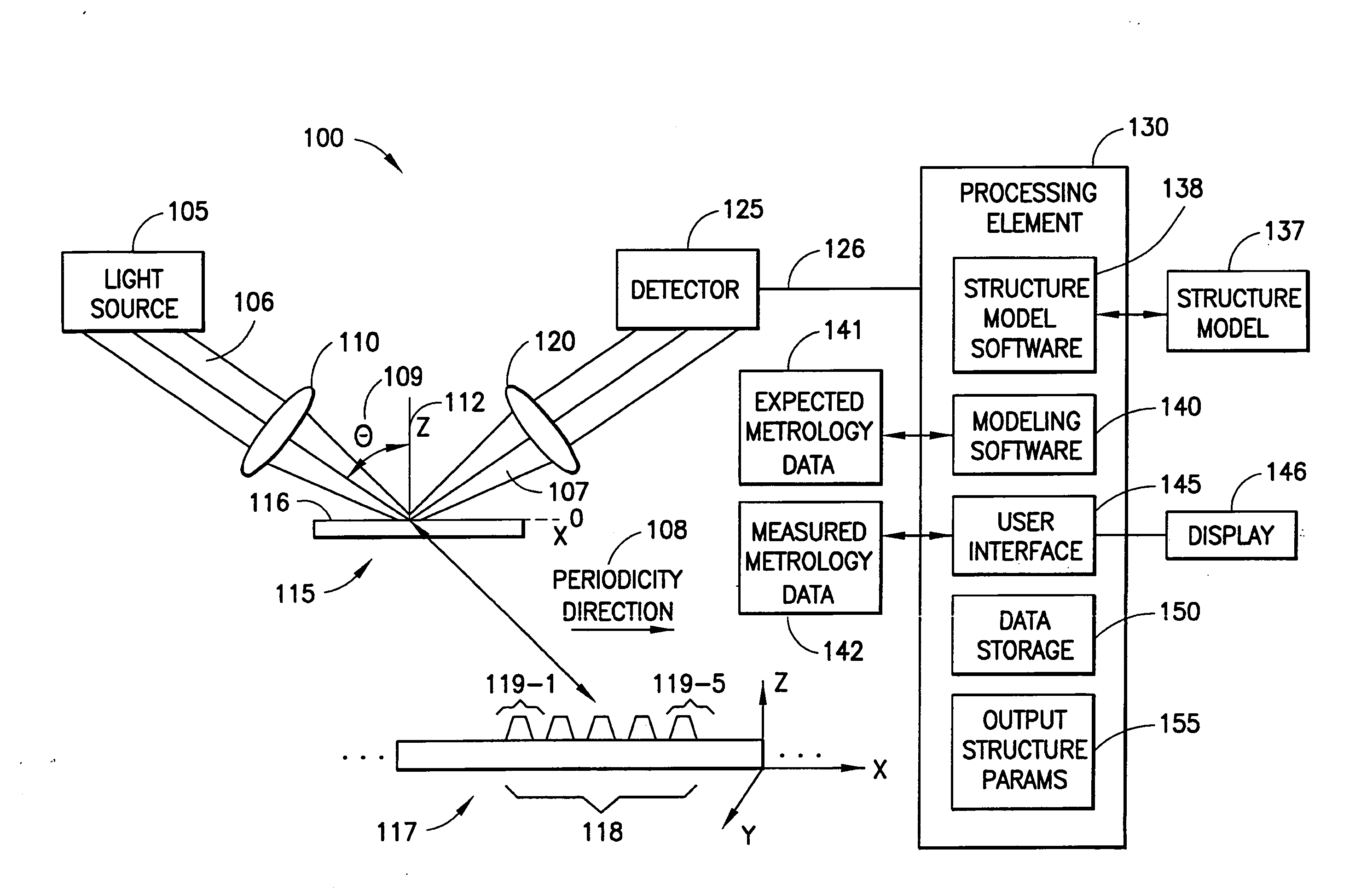
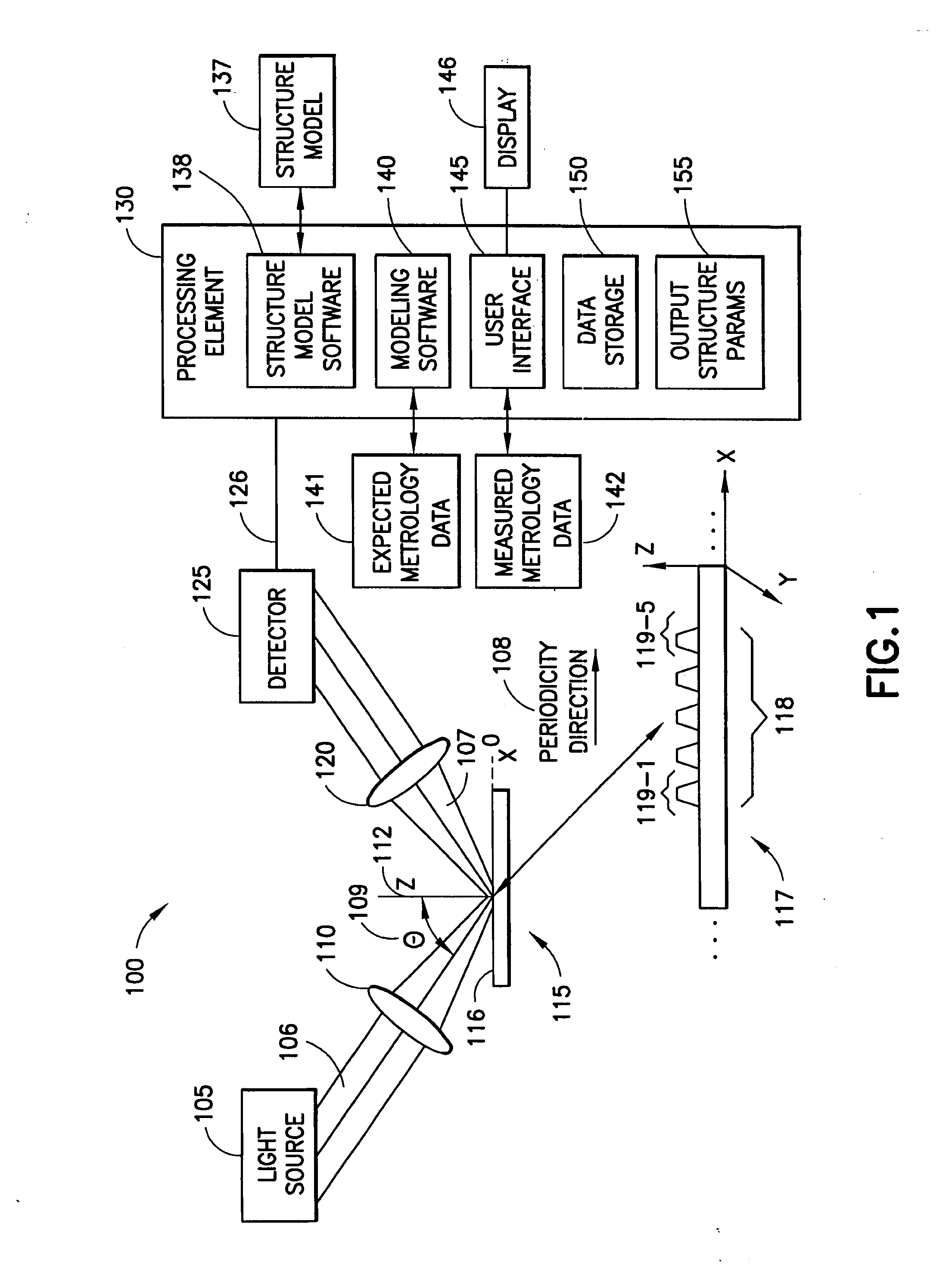
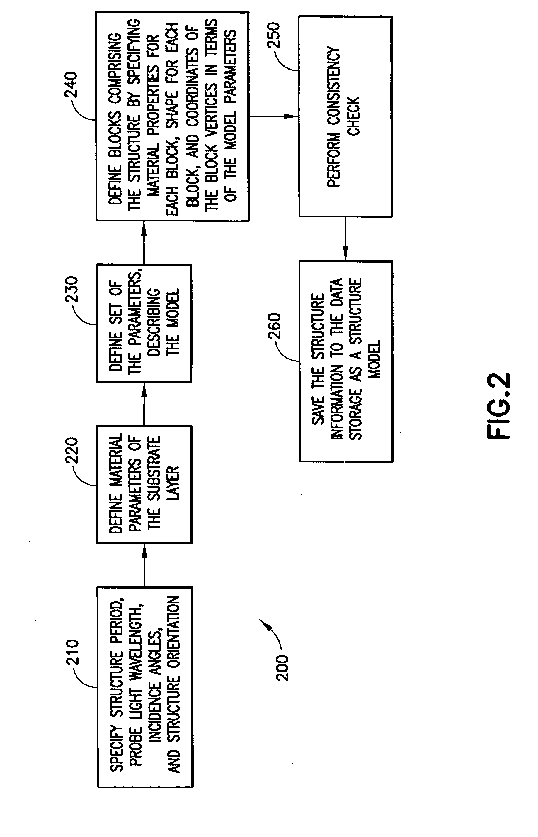
[0020]In an exemplary embodiment, a method is presented for describing and parameterizing a structure model of two-dimensional or three-dimensional periodic or standalone structures for a scattering-based metrology. Techniques are disclosed for setting up a structure model and for implementing supporting modules such as software modules. The model structure is represented as a set of blocks. In an exemplary embodiment, each block includes one material, and does not overlap with any other block. In an exemplary embodiment, material properties are assumed to be constant within a block. Blocks can assume one of a number of predefined shapes consistent with the algorithm used to calculate the solution for the scattering problem.

[0021]Further structure subdivision may be performed automatically by the software based on the information provided by describing the block shapes, positions, and constituent materials. Such structure subdivision is useful for mesh generation for finite differen...


PUM


Abstract

A method includes accessing a structure model defining a cross-sectional profile of a structure on a sample. The cross-sectional profile is at least partially defined using a set of blocks. Each of the blocks includes a number of vertices. One or more of the vertices are expressed using one or more algebraic relationships between a number of parameters corresponding to the structure. Information is evaluated from the structure model to produce expected metrology data for a scatterometry-based optical metrology. The expected metrology data is suitable for use for determining one or more of the number of parameters corresponding to the structure. Apparatus are also disclosed.

Description

TECHNICAL FIELD[0001]This invention relates generally to semiconductor metrology such as scatterometry and, more specifically, relates to modeling structures on a semiconductor in order to determine parameters of the structures.BACKGROUND[0002]Optical measurements of semiconductors and accompanying structures thereon provide fast, accurate, non-destructive, and relatively inexpensive analysis techniques. With the increasing integration density and operating frequencies of microelectronic devices, the dimensions of the basic integrated circuits (IC) components shrink, and transistor gate structures become two- and three-dimensional. As the structure dimensions become less than or comparable to light wavelengths being used in optical measurement, simple imaging like microscopy is generally not possible, and the optical measurements require analysis of the intensity and the polarization state of the light scattered off the structures on the semiconductor. Further, optical metrology mea...

Claims


Application Information

Patent Timeline
IPC IPC(8): G06F17/50
CPCG01N23/20
Inventor KOTELYANSKII, MICHAELRU, XUEPINGWOLF, ROBERT G.YANG, YUE
Owner RUDOLPH TECHNOLOGIES INC
Why Eureka
Try Eureka