Supercharge Your Innovation With Domain-Expert AI Agents!

Return loss techniques in wirebond packages for high-speed data communications

a wirebond package and high-speed data technology, applied in the direction of electrical equipment, semiconductor devices, semiconductor/solid-state device details, etc., can solve the problems of significant interference between wirebond package and return loss specifications in several high-frequency applications, increase in processing complexity, and increase in cost of flip-chip packaging, etc., to achieve the effect of reducing the amount of return loss

Inactive Publication Date: 2009-12-17
ALTERA CORP
View PDF11 Cites 1 Cited by
  • Summary
  • Abstract
  • Description
  • Claims
  • Application Information

AI Technical Summary

Benefits of technology

[0007]In accordance with another aspect of the invention, a method of reducing return loss in wirebond packaging due to wirebond inductance is detailed. The method begins by providing columns of bonding pads on a surface of a wirebond package and provides rows of die pads on a surface of an integrated circuit. The active signal lines are then connected from the die pads of the integrated circuit to the corresponding bonding pads of the wirebond package. Coplanar ground lines are disposed adjacent and on opposite sides of the active signal line. A planar distance between one of the active signal lines and the coplanar ground lines is tapered toward the bonding pads.

Problems solved by technology

The use of flipchip packaging comes at the price of increased cost and higher processing complexity.
In particular, the effect of inductance of the conductive lines in wirebond packages significantly interferes with meeting return loss specifications in several high frequency applications.
Return loss measures the amount of power that is lost due to reflections and mismatch loss in the conductive line.
Return loss is caused by impedance mismatches between the conductive lines (i.e. bondwires) and the bonding pads and the effect impedance mismatches has on signals traversing through the characteristic impedance of the conductive line.
These methods are hampered by mutual inductance between conductive lines, which limits improvement in the overall inductance.
As signal frequencies increase, return loss due to inductance of the signal line becomes a significant problem to overcome.

Method used


Image

  • Return loss techniques in wirebond packages for high-speed data communications
  • Return loss techniques in wirebond packages for high-speed data communications
  • Return loss techniques in wirebond packages for high-speed data communications

Examples


Embodiment Construction

[0017]The following embodiments describe an apparatus and method for reducing return loss in a wirebond package by reducing the inductive component in an active signal line. It will be obvious, however, to one skilled in the art, that the present invention may be practiced without some or all of these specific details. In other instances, well known process operations have not been described in detail in order not to unnecessarily obscure the present invention.

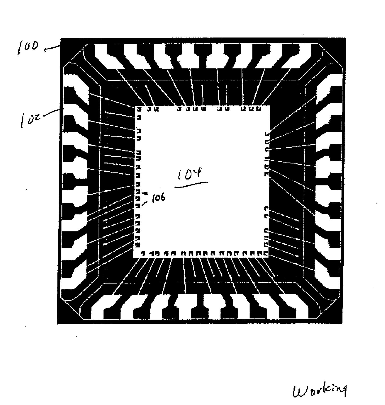
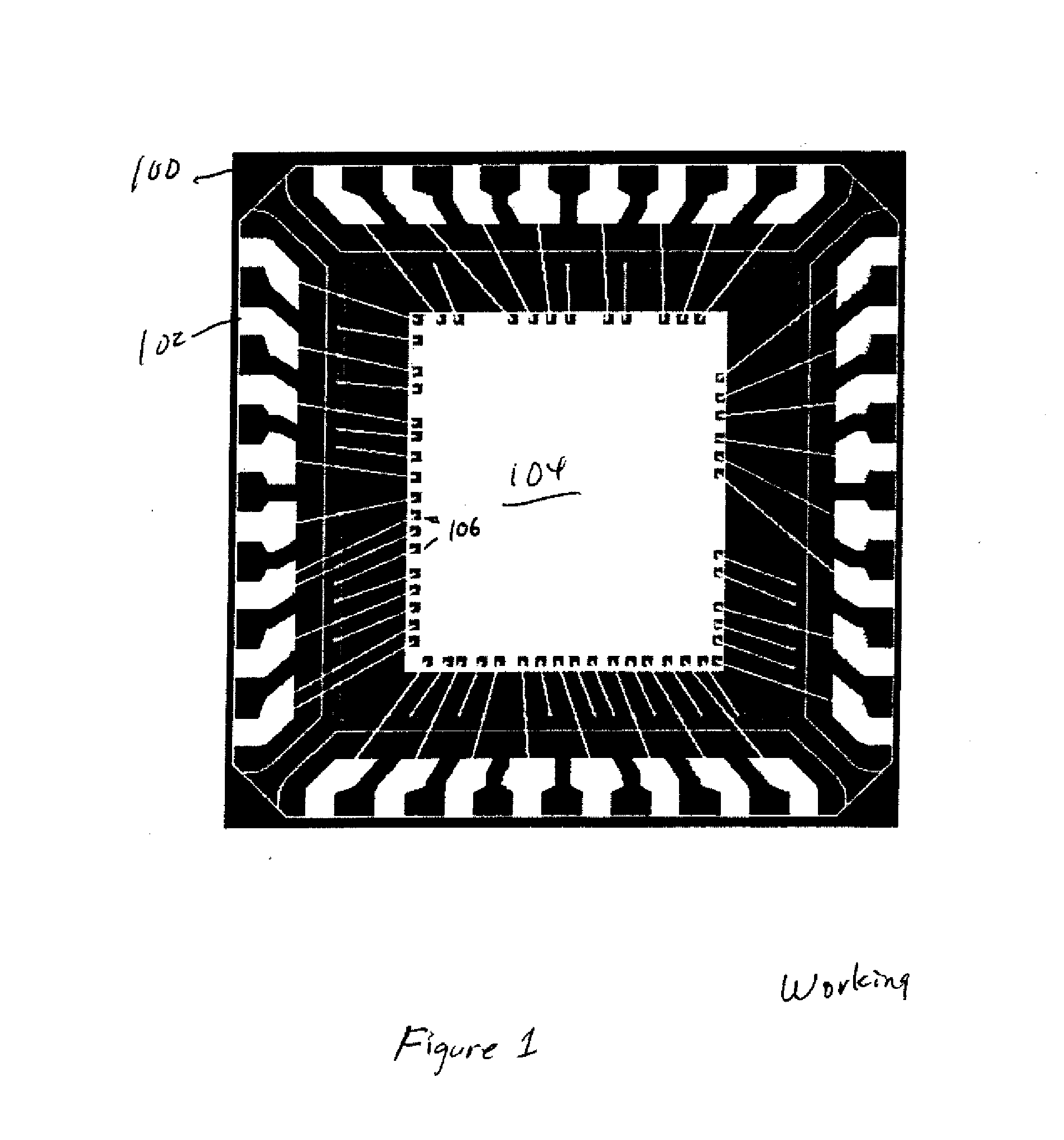
[0018]FIG. 1 illustrates a wirebond package 100 configured to reduce wirebond return loss in accordance with one embodiment of the present invention. The wirebond package is exemplary and it should be noted the following disclosure is applicable to other embodiments of wirebond packages, so long as the essential functions of providing power, ground and input signals, as well as receiving output signals from an integrated circuit are maintained. An integrated circuit 104 is generally, although not necessarily mounted in the cen...


PUM


Abstract

A wirebond package configured to reduce wirebond return loss is presented. An integrated circuit of interest with rows of bonding pads is bonded to a surface of the wirebond package. The surface of wirebond package has columns of bonding pads, which are configured to transmit or receive signals, power, and ground to and / or from the wirebond package to the integrated circuit. Corresponding die pads on the integrated circuit and bonding pads of the wirebond package are coupled using conductive lines. The conductive lines carrying the active signal has coplanar adjacent ground lines on opposing sides of active signal line and the distance between active signal line and the coplanar adjacent ground lines is tapered.

Description

BACKGROUND OF THE INVENTION[0001]Technology trends moving toward high frequency products have traditionally required the use of flipchip packaging. The use of flipchip packaging comes at the price of increased cost and higher processing complexity. If wirebond package configurations could be improved while maintaining the cost benefits over flipchip packages, several high frequency products designed for flipchip implementation could be packaged using wirebond alternatives. In particular, the effect of inductance of the conductive lines in wirebond packages significantly interferes with meeting return loss specifications in several high frequency applications.[0002]Return loss measures the amount of power that is lost due to reflections and mismatch loss in the conductive line. Return loss is caused by impedance mismatches between the conductive lines (i.e. bondwires) and the bonding pads and the effect impedance mismatches has on signals traversing through the characteristic impedan...

Claims


Application Information

Patent Timeline
Patent Type & Authority Applications(United States)
IPC IPC(8): H01L23/52
CPCH01L23/66H01L2924/19107H01L24/48H01L24/49H01L2223/6611H01L2224/45015H01L2224/48091H01L2224/48247H01L2224/484H01L2224/49113H01L2224/49171H01L2224/4943H01L2924/01033H01L2924/014H01L2924/14H01L2924/19051H01L2924/20752H01L2924/30107H01L2924/3011H01L24/02H01L2224/48257H01L2924/00014H01L2924/00H01L2924/30111H01L2224/05554H01L24/05H01L2224/49433H01L2224/45099H01L2224/05599
Inventor BEREZA, WILLIAM W.SHI, HONG
Owner ALTERA CORP
Features
  • R&D
  • Intellectual Property
  • Life Sciences
  • Materials
  • Tech Scout
  • Unparalleled Data Quality
  • Higher Quality Content
  • 60% Fewer Hallucinations
Learn More