By-pass diode structure for strings of series connected cells of a photovoltaic panel
a series connected cell and diode structure technology, applied in the field of photovoltaic panels, can solve the problems of overheating the darkened cells, reducing current yield, and overvoltage on the darkened cells that may exceed the breakdown voltage of the darkened cell,
- Summary
- Abstract
- Description
- Claims
- Application Information
AI Technical Summary
Problems solved by technology
Method used
Image
Examples
Embodiment Construction
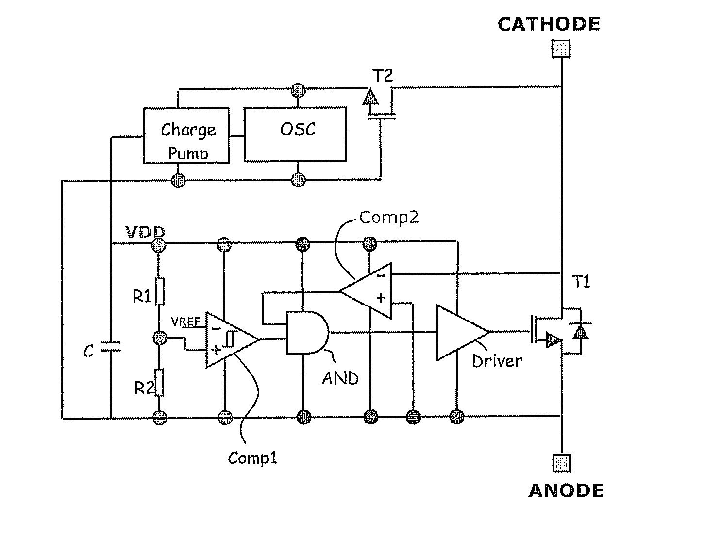
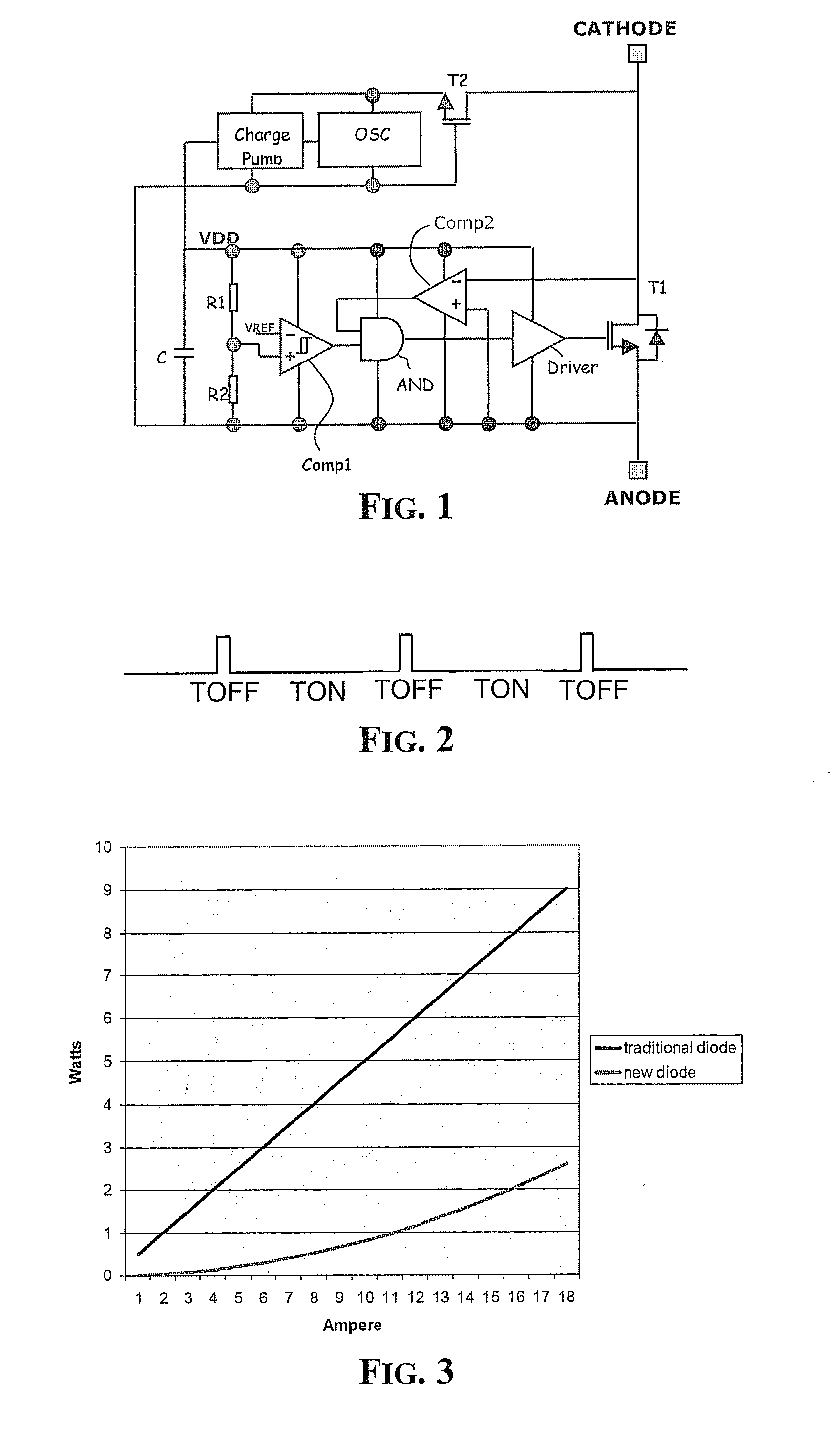
[0014]Referring to FIG. 1, an embodiment of a device is now described.
[0015]During normal functioning of a photovoltaic panel, the device is off and the voltage on the by-pass power MOS transistor T1 (between Drain and Source) that is between the cathode node (Cathode) and the anode node (Anode) of a string of cells in series, is positive.
[0016]In this normal functioning condition of the cells of the group, the MOS transistor T2 protects from high voltage the oscillator circuit normally realized with low voltage transistors. To this end, the transistor T2 may have a turn on threshold smaller than that of the intrinsic diode of the integrated structure of the MOS power transistor T1 (that is generally of about 300-400 mV).
[0017]When part of the panel and in particular the group of cells in series of the string connected between the respective cathode and anode nodes is shadowed, the current generated by other normally irradiated cells of the panel in flowing through the intrinsic dio...
PUM
 Abstract
Description
Claims
Application Information

