

Transistor having a metal nitride layer pattern, etchant and methods of forming the same
a metal nitride and layer pattern technology, applied in the field of transistors, can solve the problems of etching damage to the gate insulating deterioration of the electrical characteristics of the transistor, plasma damage to the dielectric layer and/or the semiconductor substrate, etc., to achieve the effect of reducing etching damag
- Summary
- Abstract
- Description
- Claims
- Application Information
AI Technical Summary
Benefits of technology
Problems solved by technology
Method used
Image

Examples
Embodiment Construction
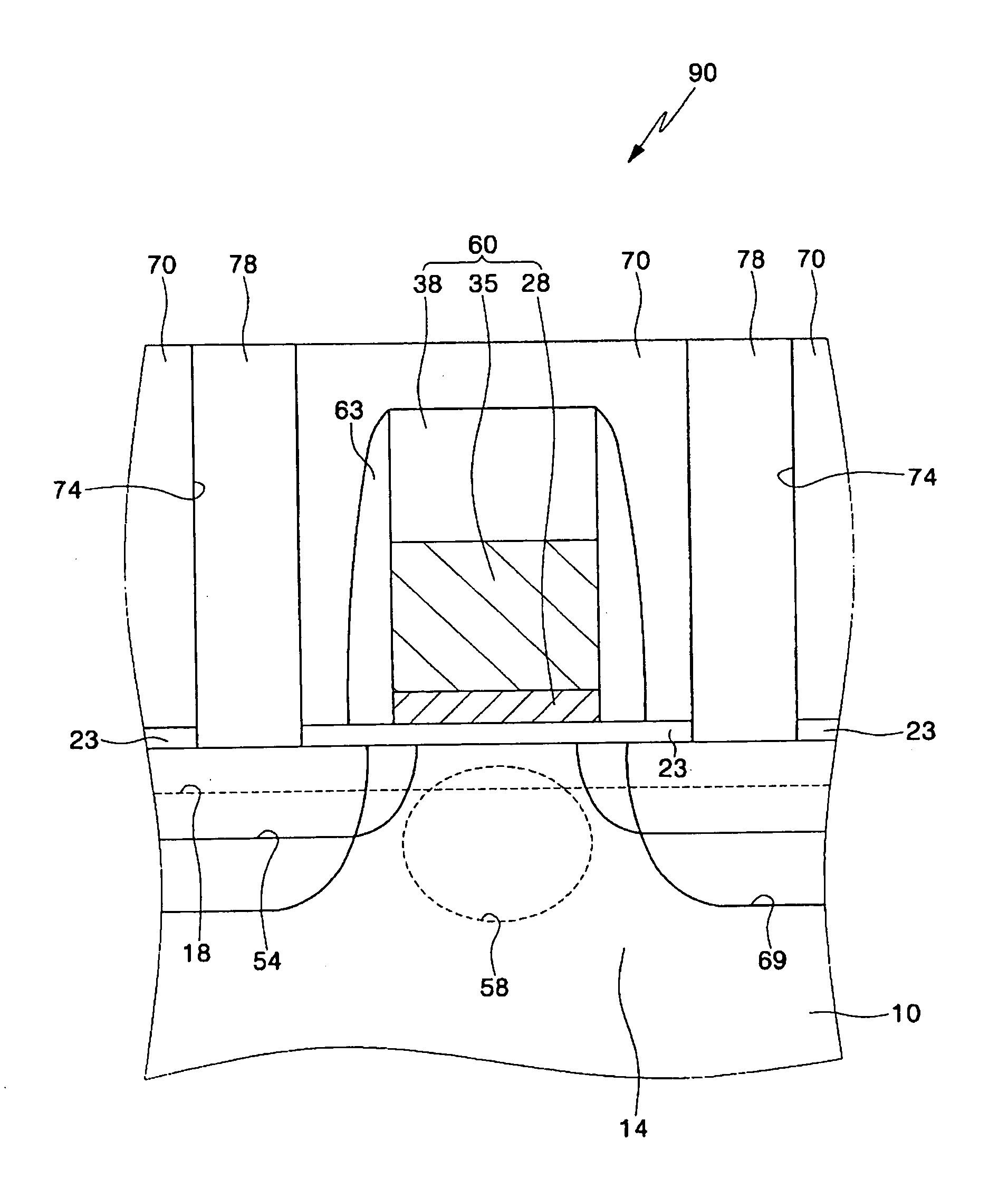
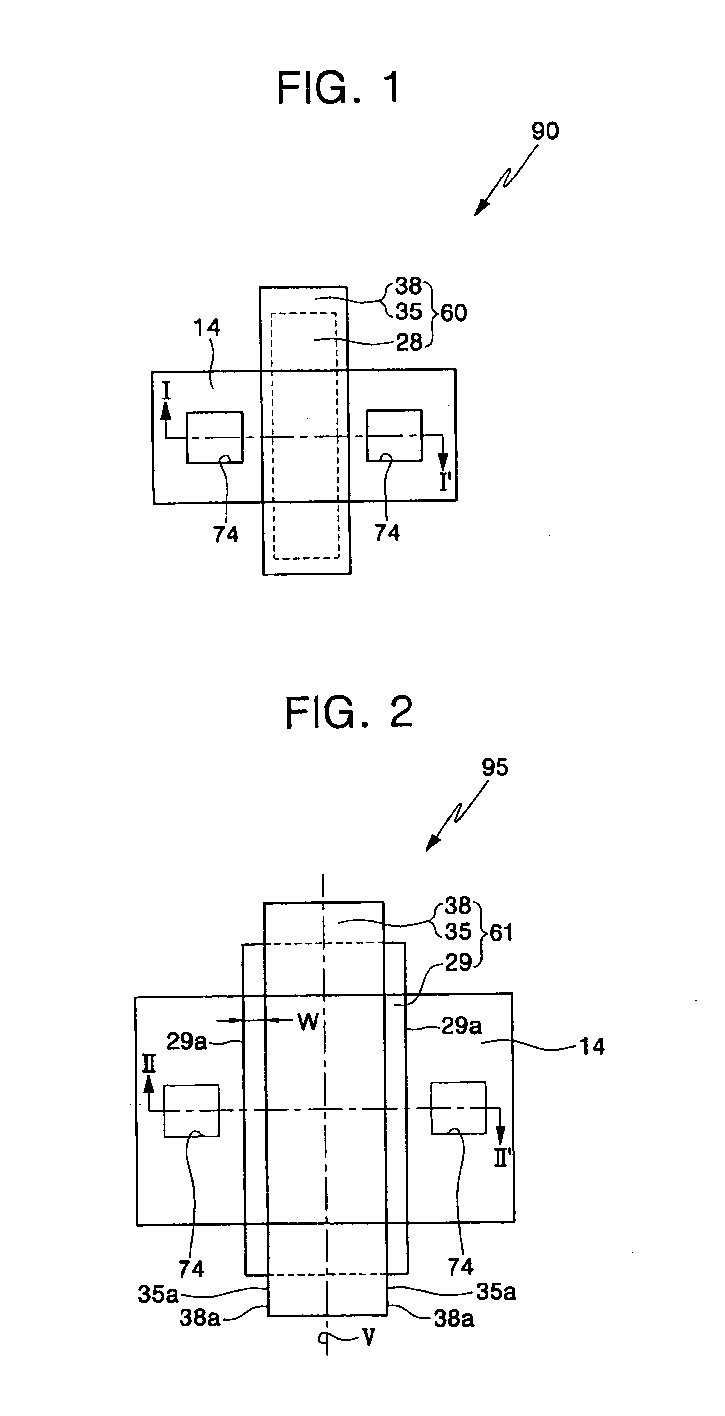
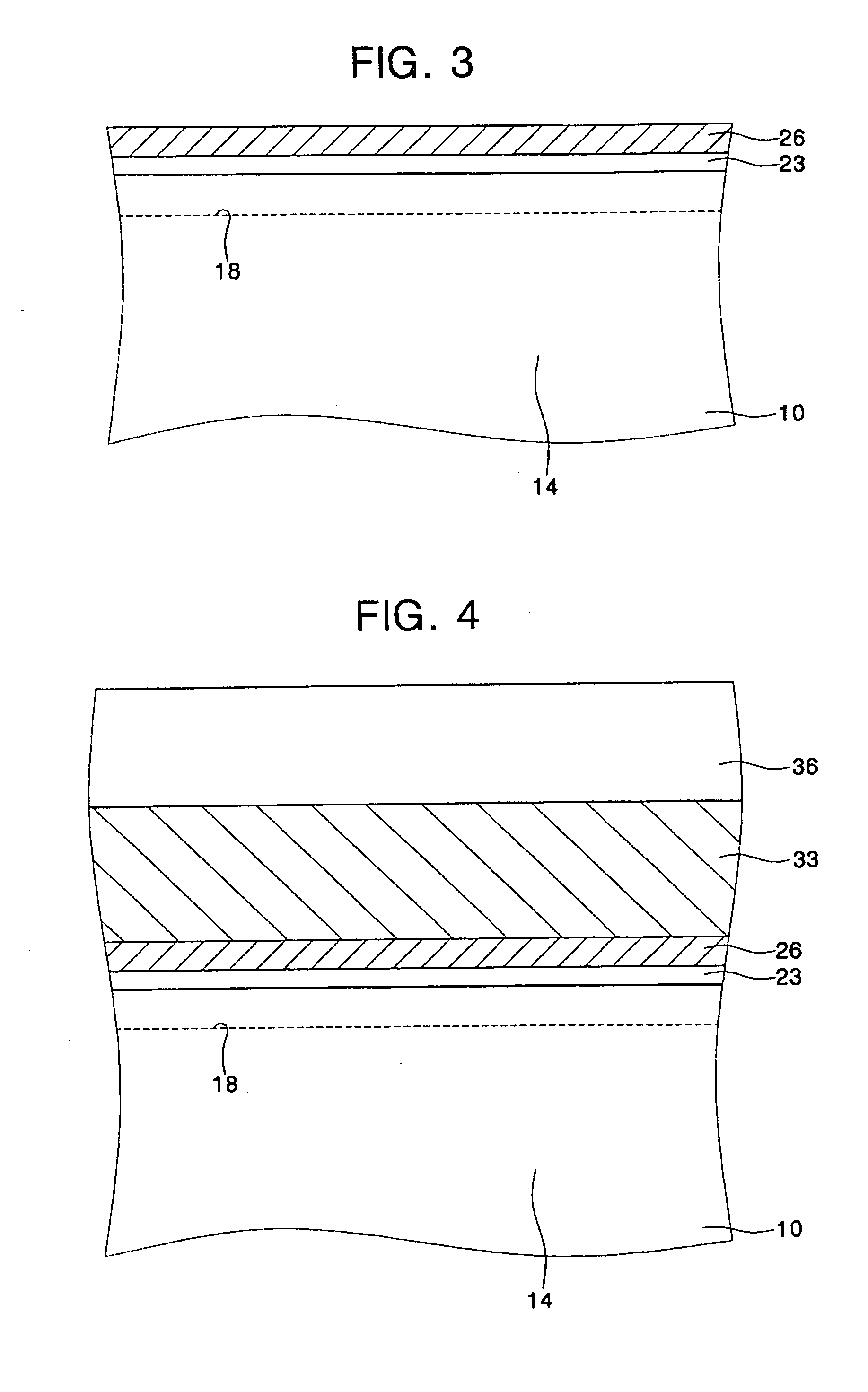
[0010]Example embodiments of the present invention provide a transistor, an etchant and methods of forming the same. Other example embodiments provide a transistor having a metal nitride layer pattern, an etchant and methods of forming the same.
[0011]According to example embodiments of the present invention, methods of forming a transistor capable of reducing etching damage to a gate insulating layer and / or a semiconductor substrate by performing an etching process with an etchant on a metal nitride layer are also provided.
[0012]According to example embodiments of the present invention, a gate insulating layer and / or a metal nitride layer may be sequentially formed on a semiconductor substrate. A gate electrode and / or a gate capping layer pattern may be sequentially formed on the metal nitride layer. An etching process may be performed on the metal nitride layer using the gate capping layer pattern and / or the gate electrode as an etching mask and / or the gate insulating layer as an e...
PUM
| Property | Measurement | Unit |
|---|---|---|
| pH | aaaaa | aaaaa |
| speed | aaaaa | aaaaa |
| thickness | aaaaa | aaaaa |
Abstract
Description
Claims
Application Information