Method for improving performance of core device and input-output device

A technology for input and output devices and core devices, applied in semiconductor devices, semiconductor/solid-state device manufacturing, electrical components, etc., can solve problems such as poor electrical performance, reduce production costs, avoid adverse effects, and reduce the number of masks. Effect

Active Publication Date: 2017-05-10
SEMICON MFG INT (SHANGHAI) CORP +1
View PDF3 Cites 3 Cited by
  • Summary
  • Abstract
  • Description
  • Claims
  • Application Information

AI Technical Summary

Problems solved by technology

[0005] However, the semiconductor devices formed by the prior art still have the problem of poor electrical performance

Method used


Image

  • Method for improving performance of core device and input-output device
  • Method for improving performance of core device and input-output device
  • Method for improving performance of core device and input-output device

Examples


Embodiment Construction

[0031] It can be known from the background technology that the electrical performance of the semiconductor device formed by the prior art is poor.

[0032] It is found through research that due to the different working voltages of the core device and the input / output device, the thickness of the gate dielectric layer of the core device and the input / output device is different. The gate dielectric layer includes an oxide layer and a high-k gate dielectric layer on the surface of the oxide layer. The thickness of the oxide layer in the core device is smaller than the thickness of the oxide layer in the input / output device, so that the thickness of the gate dielectric layer of the core device and the input / output device are different. Generally, a thicker oxide layer for the input and output devices is formed first, and then a thinner oxide layer for the core device is formed.

[0033] However, thicker oxide layers in input and output devices are susceptible to etching damage caused b...


PUM


Abstract

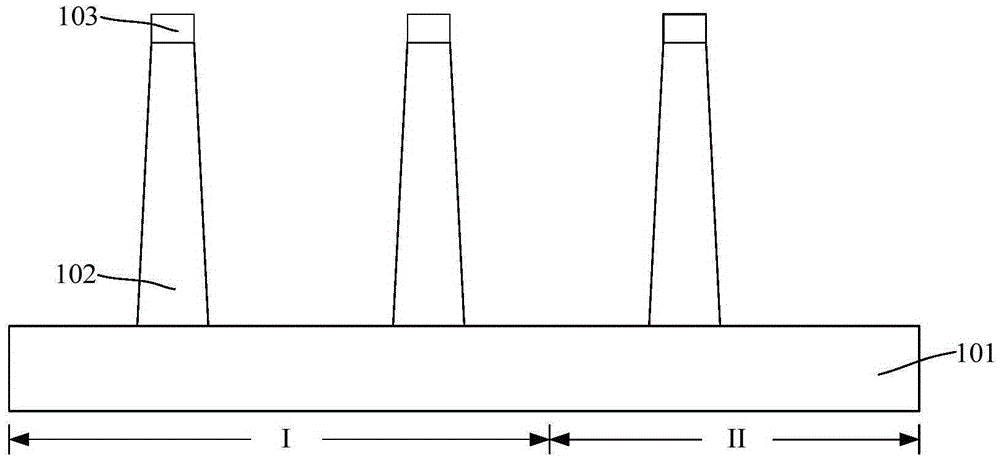
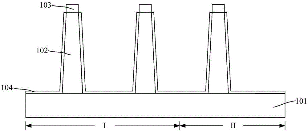
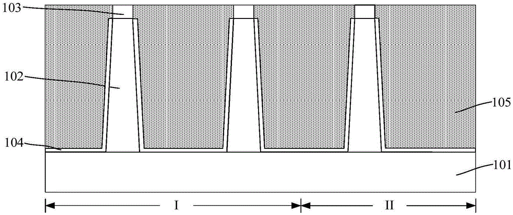
The invention provides a method for improving performance of a core device and an input-output device. The method comprises steps of providing a substrate; forming a first oxide layer on the surface of the substrate in a core device region and an input-output device region; forming a cap layer on the surface of the first oxide layer; performing etching to remove the cap layer in the core device region; forming a pseudo grid film on the surface of the cap layer in the input-output device region and the substrate in the core device region; patterning the pseudo grid film to form a pseudo grid layer; forming an interlayer dielectric layer to cover the surface of the side wall of the pseudo grid layer on the substrate after the pseudo grid layer is formed; performing etching to remove the pseudo grid layer; removing the cap layer in the input-output device region; and forming a second oxide layer on the surface of the substrate in the core device region after the cap layer is removed, wherein the thickness of the second oxide layer is smaller than the thickness of the first oxide layer. The method provided by the invention improves integrity of the grid oxide layer of the input-output device and the core device, and the NBTI performance and the PBTI performance.

Description

Technical field [0001] The invention relates to the technical field of semiconductor manufacturing, in particular to a method for improving the performance of core devices and input and output devices. Background technique [0002] Metal-Oxide-Semiconductor (MOS) devices have been called one of the commonly used semiconductor devices in integrated circuits. The MOS devices include: P-type metal oxide semiconductor (PMOS, P-type MOS) devices, N-type metal oxide semiconductor (NMOS, N-type MOS) devices, and complementary metal oxide semiconductor (CMOS, Complementary MOS) devices Device. [0003] Metal oxide semiconductor devices are mainly divided into core (Core) devices and input and output (IO, Input and Output) devices according to their functions. According to the electrical types of metal oxide semiconductor devices, core devices can be divided into core NMOS devices and core PMOS devices, and input and output devices can be divided into input and output NMOS devices and inp...

Claims


Application Information

Patent Timeline
Patent Type & Authority Applications(China)
IPC IPC(8): H01L21/8238H01L21/28
CPCH01L21/28008H01L21/823821H01L21/823857
Inventor 李勇
Owner SEMICON MFG INT (SHANGHAI) CORP
Why Eureka
Try Eureka