Mask and fabrication method thereof

A manufacturing method and mask technology, which are used in semiconductor/solid-state device manufacturing, ion implantation plating, coating, etc., can solve the problem that the quality and accuracy of the metal mask cannot meet the requirements of the process requirements, and the small Do 25μm to 40μm and other problems

Active Publication Date: 2018-10-16
NINGBO SEMICON INT CORP
View PDF4 Cites 3 Cited by
  • Summary
  • Abstract
  • Description
  • Claims
  • Application Information

AI Technical Summary

Problems solved by technology

[0004] At present, the metal mask plate of OLED (Organic Light-Emitting Diode, organic light-emitting display) is usually made of Invar alloy (INVAR, also known as Invar) with a thickness of 30 μm to 50 μm and is prepared by chemical etching. The surface of the alloy is coated with photoresist or photosensitive dry film, and the fine pattern of the mask plate is transferred to the photosensitive film by exposure, and finally a fine metal mask plate is made by means of development and chemical etching. Its precision is usually at the micron level, and generally the minimum can only be 25 μm to 40 μm, so the quality and accuracy of the metal mask made cannot well meet the requirements of the process

Method used


Image

  • Mask and fabrication method thereof
  • Mask and fabrication method thereof
  • Mask and fabrication method thereof

Examples


Embodiment Construction

[0019] It can be seen from the background art that the quality and accuracy of the metal mask cannot well meet the requirements of the process.

[0020] In order to solve the technical problem, the present invention uses semiconductor processes such as deposition, photolithography and etching to make a mask. Compared with the metal mask made by traditional chemical etching, the semiconductor process can improve the The quality of the mask plate and the accuracy of the through holes are improved, thereby improving the quality and accuracy of the mask plate, which is beneficial to improving the precision of the evaporation process.

[0021] In order to make the above objects, features and advantages of the present invention more comprehensible, specific embodiments of the present invention will be described in detail below in conjunction with the accompanying drawings.

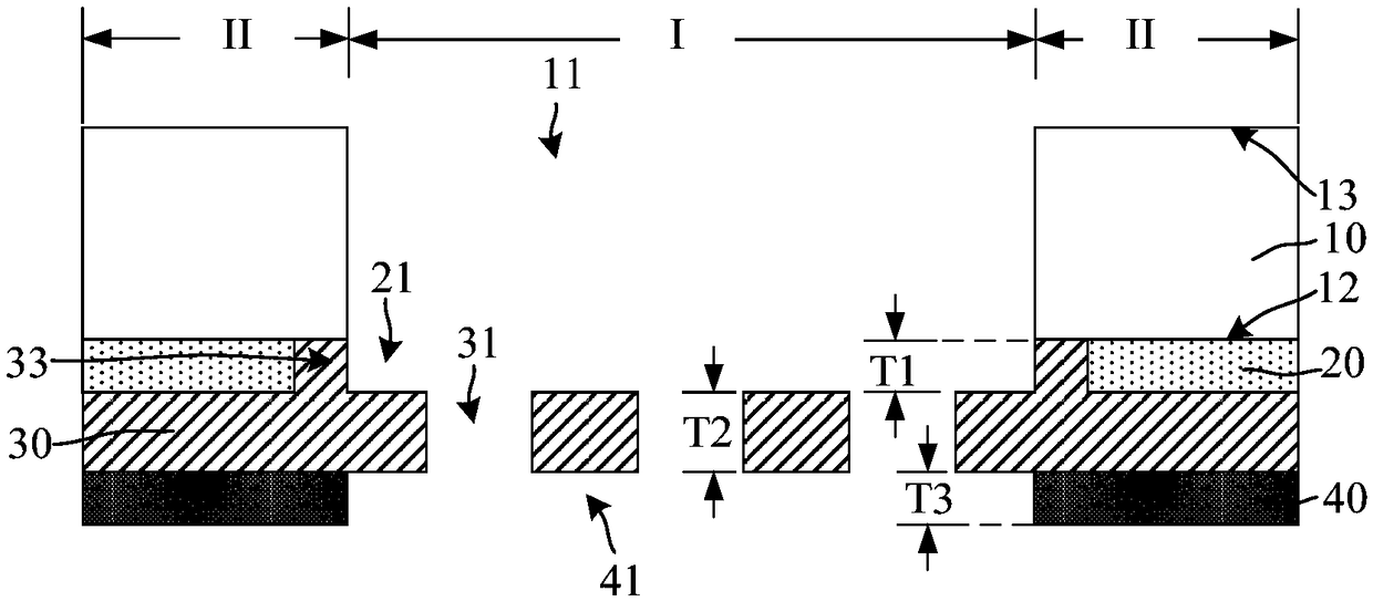
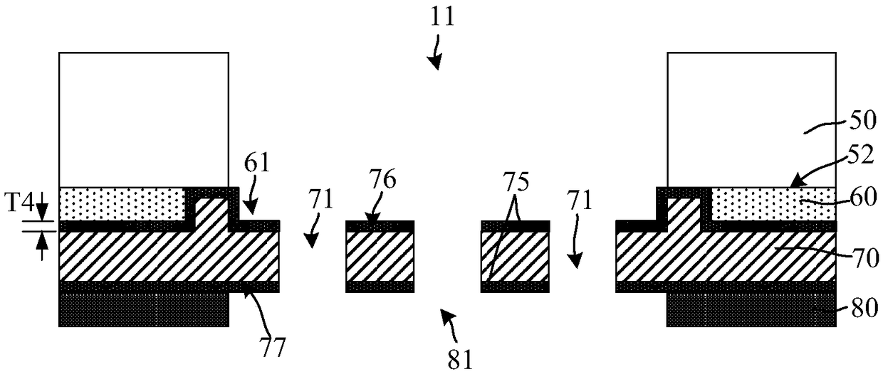
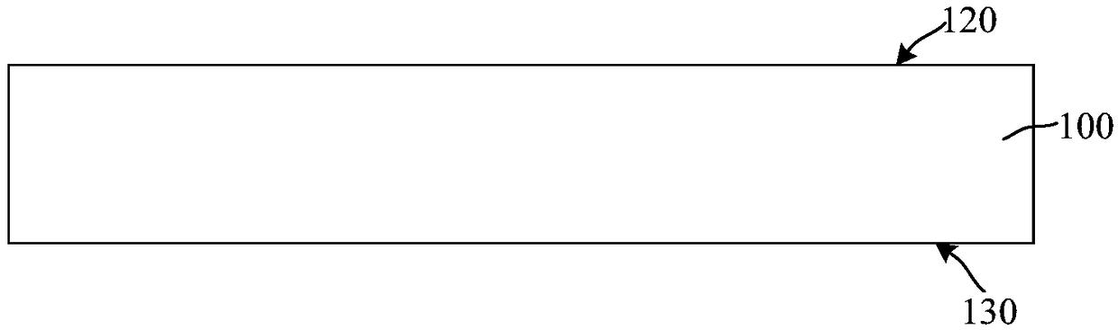
[0022] figure 1 It is a structural schematic diagram of an embodiment of the mask plate of the present inven...


PUM

PropertyMeasurementUnit
depthaaaaaaaaaa
thicknessaaaaaaaaaa

Abstract

The invention relates to a mask and a fabrication method thereof. The mask comprises a substrate, a sacrificial layer and a mask pattern layer, wherein the substrate comprises a first surface and a second surface, the second surface deviates from the first surface, a plurality of openings are formed in the substrate and penetrate through the substrate, the substrate can be used for patterning by asemiconductor etching process, the sacrificial layer is arranged on the first surface, a plurality of holes are formed in the sacrificial layer, the mask pattern layer is arranged on the sacrificiallayer and comprises pattern regions and shielding regions which are adjacent to each other, at least one through hole is formed in the pattern regions and penetrates through the mask pattern layer, the pattern regions are exposed out of the openings and holes, each pattern region is corresponding to the openings and holes, the mask pattern layer is provided with an annular bulge extending to the openings, and the annular bulge is in contact with side walls of the openings. The mask is made by the semiconductor process, the quality of the mask and the through hole accuracy can be improved by the semiconductor process, the through hole size and the thickness of the mark pattern layer are favorably reduced, displacement of the mask pattern layer and the substrate also can be prevented, and the quality and the accuracy of the mask are higher.

Description

technical field [0001] The invention relates to the field of semiconductor manufacturing, in particular to a mask plate and a manufacturing method thereof. Background technique [0002] Physical vapor deposition (Physical Vapor Deposition, PVD) technology is mainly divided into two types: evaporation (Evaporation) process and sputtering (Sputtering) process. Among them, the evaporation process is the main way to form a functional film layer on the surface of the substrate. The evaporation process refers to heating and melting the evaporation source (such as metal, alloy or compound to be plated) in a vacuum evaporation machine (Vacuum Evaporator), so that It escapes in the form of molecules or atoms, and is deposited on the surface of the substrate to form a solid film or coating. [0003] At present, the evaporation process mainly adopts a metal mask (Metal Mask), and the metal mask has openings with a preset pattern. During the evaporation process, the metal mask is fixed...

Claims


Application Information

Patent Timeline
Patent Type & Authority Applications(China)
IPC IPC(8): H01L51/56C23C14/04
CPCC23C14/042H10K71/164H10K71/166
Inventor 刘孟彬罗海龙
Owner NINGBO SEMICON INT CORP
Why Eureka
Try Eureka