Method of manufacturing thin film transistor, thin film transistor, and display unit

a technology of thin film transistors and display units, which is applied in the direction of transistors, solid-state devices, semiconductor devices, etc., can solve the problems of reducing on-characteristics, generating unnecessary compounds, and destroying the crystalline silicon film forming the channel region

Inactive Publication Date: 2010-02-18
SONY GRP CORP
View PDF5 Cites 6 Cited by
  • Summary
  • Abstract
  • Description
  • Claims
  • Application Information

AI Technical Summary

Benefits of technology

[0015]To reduce the etching residue of the buffer layer, for example, the following methods are effective. That is, after treatment with hydrogen fluoride solution, water washing treatment is made. Otherwise, before forming the upper layer of the buffer layer by CVD (Chemical Vapor Deposition) method, plasma treatment is made by using an etching gas such as hydrogen and argon in a CVD chamber. However, even in the foregoing methods, the crystalline silicon film as a channel is damaged, and when the treatment is made excessively, the on-current is lowered.
[0019]In the method of manufacturing a thin film transistor of the embodiment of the invention, the heat treatment is indirectly provided through the photothermal conversion layer and the first insulating layer. Therefore, heat is uniformly transferred to the first amorphous silicon film to form the crystalline silicon film. Further, since the first insulating layer is formed between the first amorphous silicon film and the photothermal conversion layer, a product is not generated due to reaction thereof. After that, the photothermal conversion layer is removed, the first insulating layer is patterned to selectively leave only the region thereof corresponding to the channel region, and thereby such region becomes the channel protective film. At this time, since the portion to become the channel protective film is not removed, the channel region in the crystalline silicon film as a lower layer is protected and is not damaged. After that, as an upper layer of the channel protective film, the n+ silicon film and the metal film are formed, and the region thereof corresponding to the channel region is selectively removed, and thereby the source region, the drain region, the source electrode, and the drain electrode are respectively formed. The channel protective film functions as the etching stopper. Therefore, the channel region of the crystalline silicon film is protected and is not damaged.
[0020]In the method of manufacturing a thin film transistor according to the embodiment of the invention, it is preferable that a step of forming a second insulating layer on the first insulating layer is included after the step of removing the photothermal conversion layer. It is preferable that the first and the second insulating layers are patterned to selectively leave only a region corresponding to the channel region, and thereby the channel protective film is formed. In this case, the film thickness of the channel protective film functioning as the etching stopper becomes large. Therefore, the channel region of the crystalline silicon film is more surely protected.
[0025]According to the method of manufacturing a thin film transistor, the thin film transistor, and the display unit of the embodiment of the invention, the crystalline silicon film is formed by the heat treatment through the photothermal conversion layer and the insulating film (first insulating film). In addition, the channel protective film is selectively formed in the region corresponding to the channel region on the crystalline silicon film by patterning the insulating film. Therefore, crystallization can be made by the indirect heat treatment. In addition, when the insulating film is peeled, the channel protective film can mask the channel region of the crystalline silicon film, and when the n+ silicon film and the metal film are selectively removed, the channel protective film can function as the etching stopper. Therefore, when the crystalline silicon film is formed, heat can be uniformly supplied, the channel region of the crystalline silicon film can be protected, and the characteristics variation of the thin film transistor can be inhibited without deteriorating the characteristics thereof.

Problems solved by technology

However, when such a photothermal conversion layer is used, it is often the case that at a high temperature (at least 1410 degree C. that is the melting point of silicon), the photo thermal conversion layer and the silicon film are reacted, and thus an unnecessary compound is generated.
In addition, the crystalline silicon film forming the channel region is damaged, and the on-characteristics are lowered.
However, even in the foregoing methods, the crystalline silicon film as a channel is damaged, and when the treatment is made excessively, the on-current is lowered.

Method used


Image

  • Method of manufacturing thin film transistor, thin film transistor, and display unit
  • Method of manufacturing thin film transistor, thin film transistor, and display unit
  • Method of manufacturing thin film transistor, thin film transistor, and display unit

Examples


first embodiment

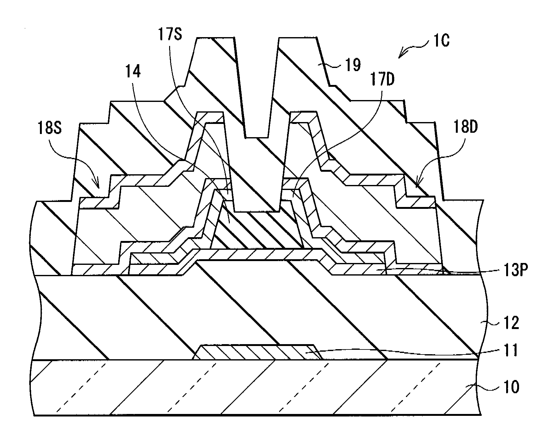
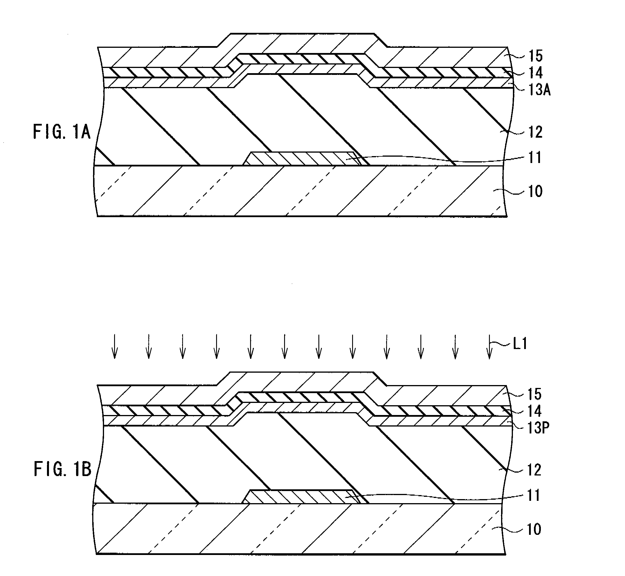
[0041]FIG. 1A to FIG. 5B are views for explaining a method of manufacturing a thin film transistor (thin film transistor 1) according to a first embodiment of the invention.

[0042]First, as shown in FIG. 1A, a gate electrode 11, a gate insulating film 12, an amorphous silicon film 13A (first amorphous silicon film), a buffer layer 14 (first insulating film), and a photothermal conversion layer 15 are formed in this order over an insulative substrate 10 made of a glass material and a plastic material.

[0043]More specifically, the gate electrode 11 is formed as follows. A molybdenum (Mo) film being about 100 nm thick is uniformly formed on the substrate 10 by, for example, sputtering method. After that, the molybdenum film is etched and patterned in a given shape. The patterning into such a given shape is made by, for example, photolithography method or the like. The gate electrode 11 is not necessarily made of Mo, but may be made of a metal with the high melting point that is hardly al...

second embodiment

[0066]Next, a description will be given of a method of manufacturing a thin film transistor (thin film transistor 1A) according to a second embodiment of the invention. Elements identical with the elements in the first embodiment are affixed with the identical symbol, and the description thereof will be omitted as appropriate.

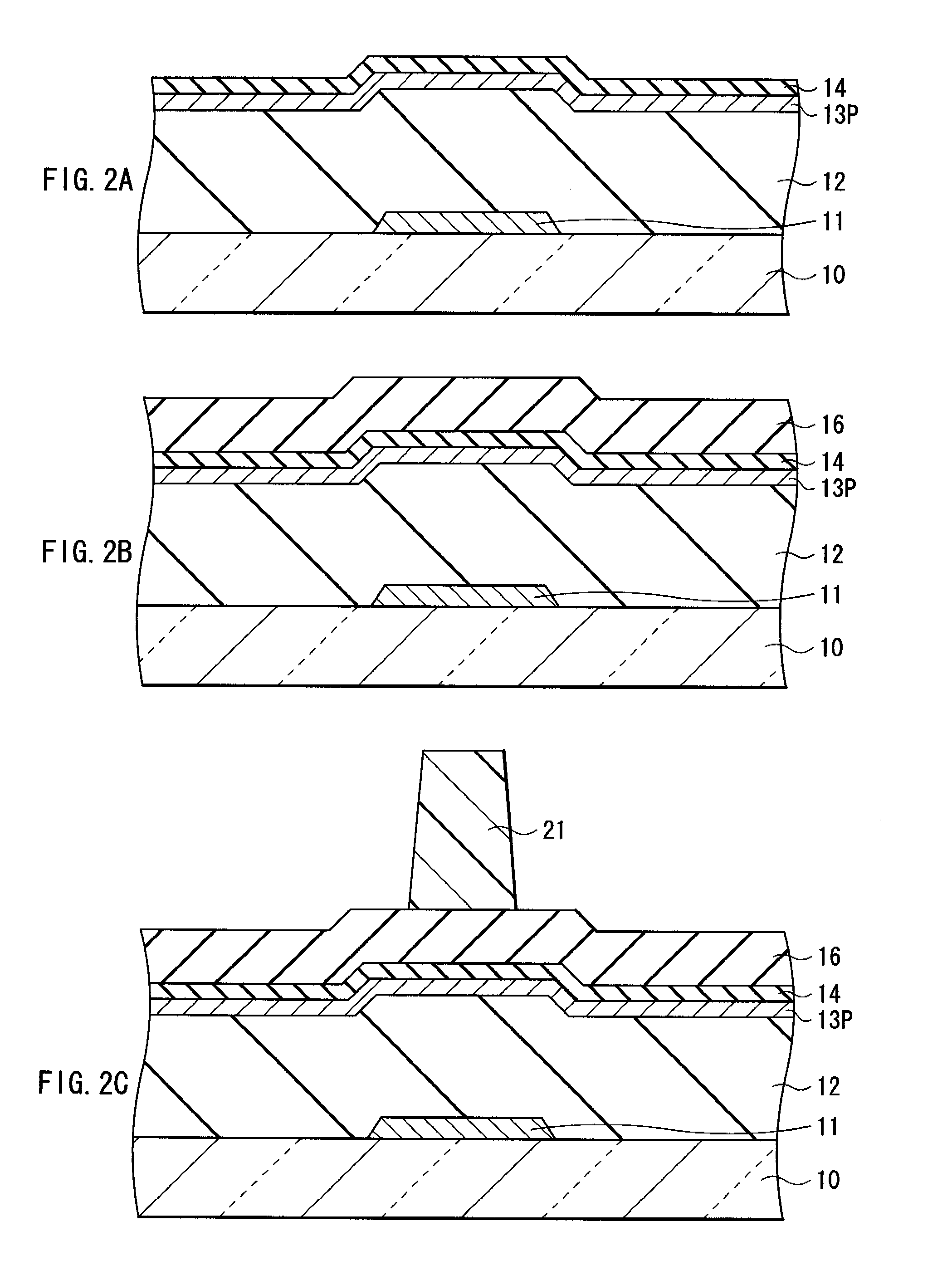
[0067]First, as shown in FIG. 10A, in the same manner as in the thin film transistor 1 of the first embodiment, the gate electrode 11, the gate insulating film 12, the amorphous silicon film 13A, the buffer layer 14, and the photothermal conversion layer 15 are sequentially formed over the substrate 10. Next, the photothermal conversion layer 15 is uniformly irradiated with the laser beam L1, and heat treatment is indirectly provided for the amorphous silicon film 13A, and thereby the crystalline silicon film 13P is formed. Next, in the same manner as in the thin film transistor 1, the buffer layer 14 and the insulating film 16 are patterned to form the channel...


PUM


Abstract

A thin film transistor having a crystalline silicon film that is formed over an insulating substrate with a gate electrode and a gate insulating film in between, and has a channel region in a region corresponding to the gate electrode; an insulating channel protective film that is selectively formed in a region corresponding to the channel region on the crystalline silicon film; an n+ silicon film having a source region and a drain region that sandwich a region corresponding to the channel region on the channel protective film and the crystalline silicon film; and a metal film having a source electrode and a drain electrode that respectively correspond to the source region and the drain region.

Description

RELATED APPLICATION DATA[0001]This application is a division of U.S. patent application Ser. No. 11 / 744,299, filed May 4, 2007, the entirety of which is incorporated herein by reference to the extent permitted by law. The present invention contains subject matter related to Japanese Patent Application JP 2006-131056 filed in the Japanese Patent Office on May 10, 2006, the entire contents of which are incorporated herein by reference to the extent permitted by law.BACKGROUND OF THE INVENTION[0002]1. Field of the Invention[0003]The present invention relates to a method of manufacturing a thin film transistor in which an amorphous silicon film is crystallized by using heat treatment with a laser beam, a thin film transistor obtained with the use of such crystallization, and a display unit including such a thin film transistor.[0004]2. Description of the Related Art[0005]In these years, as one of flat panel displays, an organic EL display unit that displays images by using organic EL (E...

Claims


Application Information

Patent Timeline
Patent Type & Authority Applications(United States)
IPC IPC(8): H01L33/00H01L29/786H01L21/20H01L21/336H01L51/50
CPCH01L21/2026H01L27/12H01L27/1281H01L29/78678H01L29/66765H01L21/02683H01L21/02686H01L21/02422H01L21/02488H01L21/02491H01L21/02502H01L21/02496H01L21/02532H01L21/02675H01L21/02667
Inventor ARAI, TOSHIAKIINAGAKI, YOSHIO
Owner SONY GRP CORP
Why Eureka
Try Eureka