Device and control method of device

a control method and device technology, applied in pulse generators, pulse techniques, instruments, etc., can solve the problem of not being able to use as the latency counter of sdram

Active Publication Date: 2010-03-04
LONGITUDE LICENSING LTD
View PDF7 Cites 33 Cited by
  • Summary
  • Abstract
  • Description
  • Claims
  • Application Information

AI Technical Summary

Benefits of technology

[0008]In one embodiment, there is provided a device that includes at least: a first control circuit receiving a first signal in response to a first clock and generating a second signal; and a second control circuit receiving the second signal in response to a second clock which leads in phase from the first clock, outputting a third signal to an output node thereof and including a divider which has a variable divide ratio, the second control circuit controlling an output timing at which the second control circuit outputs the third signal in response to the variable divide ratio.
[0009]Moreover, in another embodiment, there is provided a device that includes at least: a clock generating circuit receiving an external clock and generating a first internal clock, the first internal clock delayed in phase from the external clock; a DLL circuit receiving the external clock and generating a second internal clock, the second internal clock leading in phase to the external clock; a first contr

Problems solved by technology

For this reason, since the latency between change clocks cannot b

Method used


Image

  • Device and control method of device
  • Device and control method of device
  • Device and control method of device

Examples


first embodiment

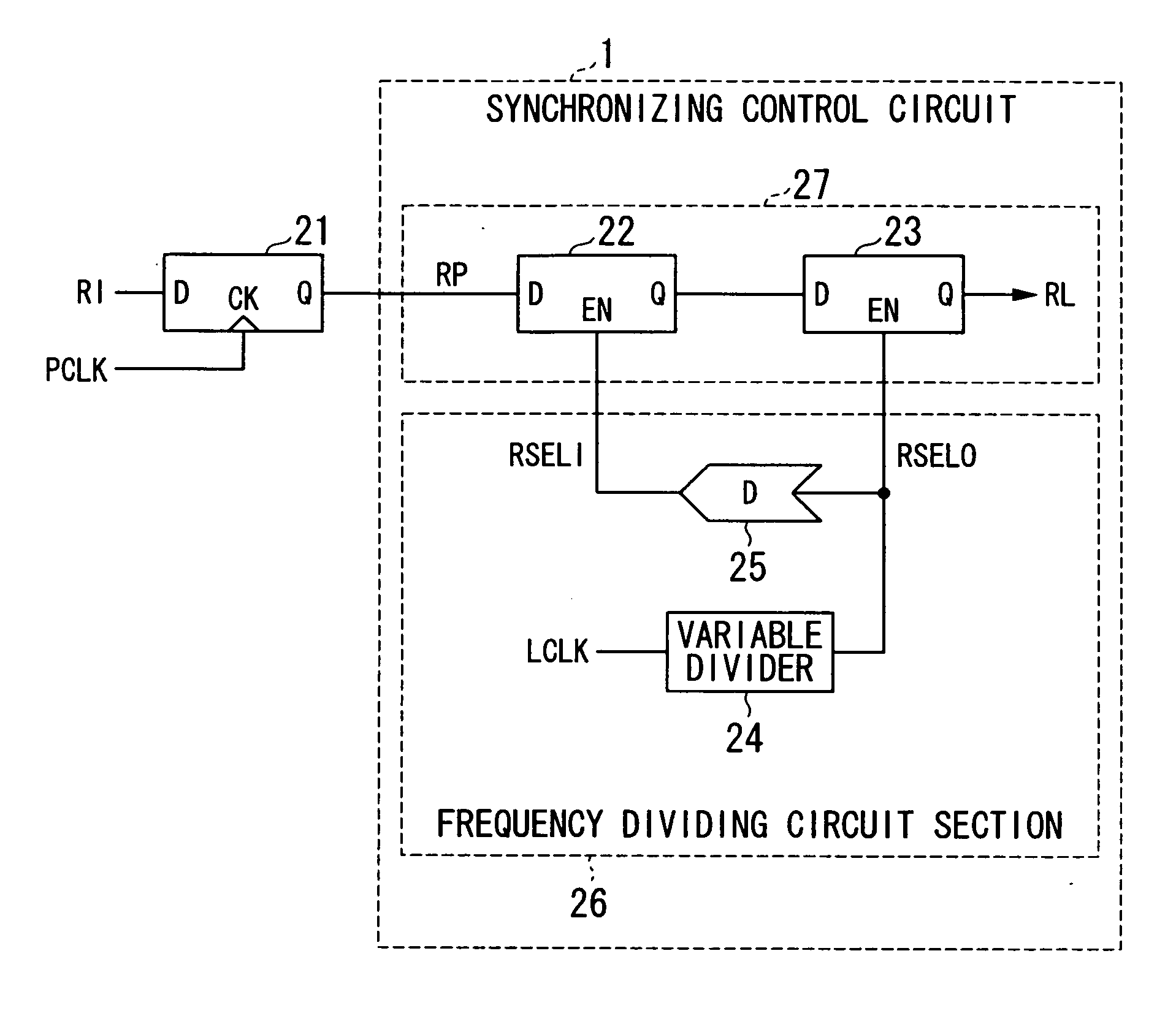
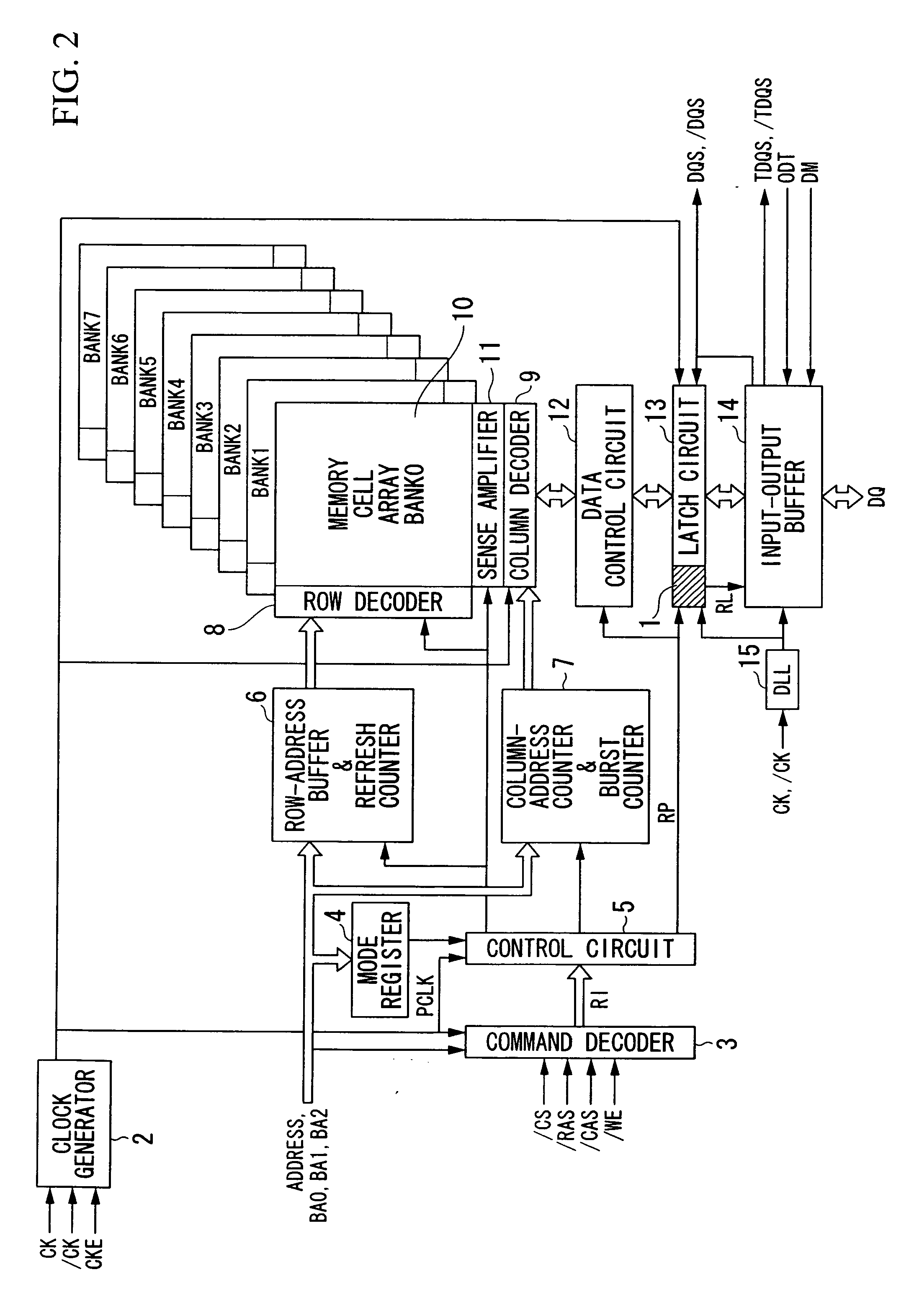
[0022]Hereinafter, embodiments of the invention will be described with reference to the accompanying drawings. FIG. 1 is a block diagram illustrating the configuration of a synchronization control circuit 1 according to the invention, and FIG. 2 is a block diagram illustrating the configuration of an SDRAM in which the synchronization control circuit 1 is used.

[0023]First, the SDRAM will be described. Referring to FIG. 2, reference numerals 2, 3, 4, and 5 denote a clock generator, a command decoder, a mode register, and a control circuit, respectively. Reference numeral 6 denotes row address buffer & refresh counter, and reference numeral 7 denotes column address counter & burst counter. Reference numerals 8, 9, 10, and 11 denote a row decoder, a column decoder, a memory cell array, and a sense amplifier, respectively. Reference numerals 12, 13, 14, and 15 denote a data control circuit, a latch circuit, an input / output buffer, and a DLL (Delay Locked Loop), respectively.

[0024]In the...

second embodiment

[0043]Next, the invention will be described.

[0044]FIG. 7 is a circuit diagram illustrating the configuration of a synchronization control circuit 1a according to the present embodiment. The present embodiment is an embodiment corresponding to continuous Read command input (refer to FIG. 9).

[0045]In FIG. 7, the clock PCLK is an internal clock which is delayed from the external clock CK (which lags behind the external clock CK in phase). The command RI is an internal Read command obtained by decoding an external command, / CS, / RAS, / CAS, and / WE. The internal Read command RI is read into a D flip-flop 21 by the internal clock PCLK and is then output as the signal RP to latches 22-1 to 22-4 of the synchronization control circuit 1a. The latches 22-1 to 22-4 read a signal RP in response to a delayed frequency-divided clock RSELI output from the delay circuits 25-1 to 25-4 and output it to latches 23-1 to 23-4. The latches 23-1 to 23-4 read the outputs of the latches 22-1 to 22-4 in resp...


PUM


Abstract

A frequency divider section generates a frequency-divided clock RSELO by dividing the frequency of an internal clock LCLK, which lags behind an external clock in phase, and generates a delayed frequency-divided clock RSELI by delaying the frequency-divided clock RSELO. A signal input from the outside in synchronization with an internal clock PCLK which lags behind the external clock in phase is held in a latch circuit in synchronization with the delayed frequency-divided clock RSELI. Then, an output signal of the latch circuit is read into a latch circuit in synchronization with the frequency-divided clock RSELO and is output as a signal which is synchronized with the internal clock LCLK. In addition, a frequency divider section includes a variable divider which divides the frequency of the internal clock LCLK by a predetermined divide ratio which can be changed.

Description

BACKGROUND OF THE INVENTION[0001]1. Field of the Invention[0002]The present invention relates to a synchronization control circuit used for the synchronization of an external clock and an internal clock, a semiconductor device using the synchronization control circuit, and a control method of the synchronization control circuit.[0003]Priority is claimed on Japanese Patent Application No. 2008-219744, filed Aug. 28, 2008, the content of which is incorporated herein by reference.[0004]2. Description of Related Art[0005]An SDRAM having a DLL (Delay Locked Loop) is controlled by using two internal clocks of an internal clock PCLK, which is delayed from an external clock CK (which lags behind the external clock CK in phase), and an internal clock LCLK, which leads the external clock CK (which leads the external clock CK in phase). Here, the internal clock PCLK is a clock obtained when the external clock CK is delayed due to a wiring line and the like in the SDRAM. On the other hand, the ...

Claims


Application Information

Patent Timeline
IPC IPC(8): H03B19/00H03L7/06G11C7/22
CPCG11C7/1072G11C7/22H03L7/0812G11C11/4076H03K23/667G11C7/222
Inventor SHIBATA, TOMOYUKI
Owner LONGITUDE LICENSING LTD
Why Eureka
Try Eureka