Chip-Stacked Package Structure and Method for Manufacturing the Same

a technology of stacked packages and packaging, which is applied in the direction of semiconductor devices, semiconductor/solid-state device details, electrical apparatus, etc., can solve the problems of reducing the manufacture yield, reducing the design flexibility and the number of chips stacked in a single package, and increasing the thickness of the pancake structure. , to achieve the effect of reducing the length reducing the size of the upper chip, and extending the length and the radian of the bonding wir

Inactive Publication Date: 2010-04-22
CHIPMOS TECH INC
View PDF8 Cites 7 Cited by
  • Summary
  • Abstract
  • Description
  • Claims
  • Application Information

AI Technical Summary

Benefits of technology

[0014]In accordance with above descriptions, the features of the present invention are providing a patterned circuit layer disposed on a rear surface of a lower chip in a chip-stacked package structure, wherein the patterned circuit layer has at least one finger (or through hole) electrically connected to at least one bonding pad (or solder) disposed on the upper chip that is stacked thereon. Accordingly, it is not necessary to extend the length and the radian of the bonding wire in connecting the upper chips with the substrate or to reduce the size of the upper chip for involving more chips in a single package, so as to solve the prior problems in the art. Also, since the lengths of wires are reduced, the disadvantage of wire sweep also can be improved.
[0015]By means of stacking the chips on the substrate with via plug instead of bonding wires for electrically connecting the chips to the substrate in the chip-stacked package structure, the embodiments of the present invention have the advantage of enhancing the heat radiation, improving the electrical connection between the substrate and the chips, and reducing the whole volume of the chip-stacked package structure.

Problems solved by technology

Thus the design flexibility and the number of chips stacked in a single package are limited.
Consequently, when a subsequent stamping process is conducted, the bonding wires may be wrenched off so as to make the electrical connection short and to decrease its manufacture yield.
However, using the dummy can increase the thickness of the pancake structure and may conflict with the trend of package size minimization.

Method used


Image

  • Chip-Stacked Package Structure and Method for Manufacturing the Same
  • Chip-Stacked Package Structure and Method for Manufacturing the Same
  • Chip-Stacked Package Structure and Method for Manufacturing the Same

Examples


fourth embodiment

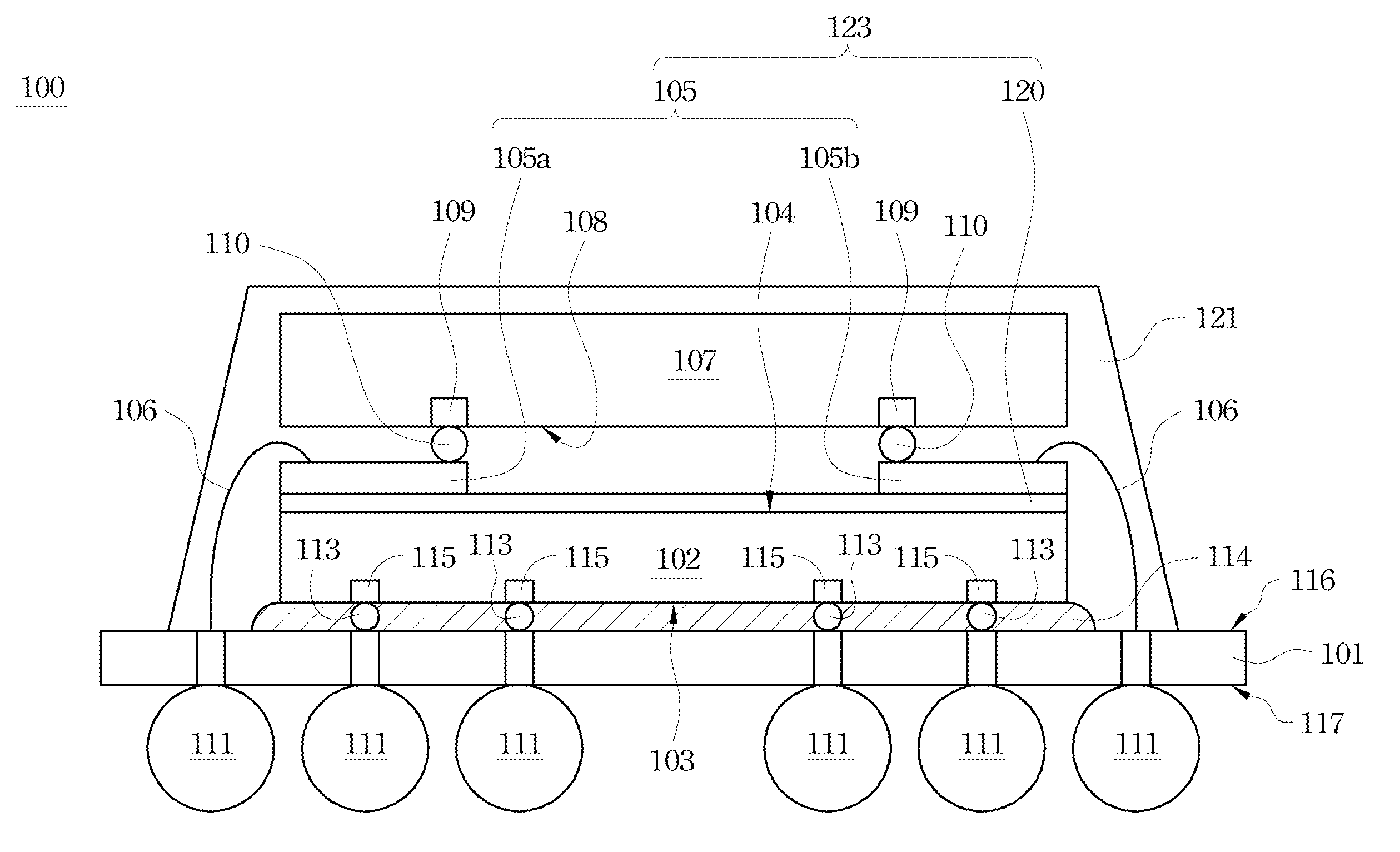
[0055]Referring to FIG. 4, FIG. 4 illustrates a chip-stacked package structure 400 according to the present invention. The chip-stacked package structure 400 includes a main substrate 400a, a first baseboard substrate 400b, and a molding compound 421. The main substrate 400a includes a substrate 401, and a first chip 402. The first baseboard substrate 400b has a third surface 416a and a fourth surface 417a. The fourth surface 417a faces towards the substrate 401.

[0056]The substrate 401 has a first surface 416 and a second surface 417 opposite to the first surface 416. The substrate 401 includes a first bonding pad 420c, a second bonding pad 420d. In some embodiments of the present invention, the substrate 401 can be a lead frame, a printed circuit board or a die carrier. In the present embodiment, the substrate 401 is a printed circuit board made of FR4 or BT epoxy, or made of the materials that constitute a flexible printed circuit board. The first bonding pad 420c and the second b...

fifth embodiment

[0061]Referring to FIG. 5, FIG. 5 illustrates a chip-stacked package structure 500 according to the present invention. The chip-stacked package structure 500 is similar to the chip-stacked package structure 400, except that the chip-stacked package structure 500 further includes a second baseboard substrate 400c. The second baseboard substrate 400c has a structure identical to the structure of first baseboard substrate 400b. There is no further statement here. However, a package structure with four or more chips should also fall within the scope and spirit of the embodiments of the present invention.

[0062]Although FIG. 5 is shown and described as having certain numbers and types of elements, such as patterned circuit layers, via plugs or bonding pads, exemplary embodiments are not so limited; that is, other embodiments may include elements other than the ones shown, and may also include different numbers of the elements than are shown. The person skilled in the art should be assumed...


PUM


Abstract

A chip stacked package structure and applications are provided. The chip-stacked package structure includes a main substrate, a baseboard substrate, and a molding compound. The main substrate has a substrate and a first chip. The substrate has a first surface and a second surface opposite to the first surface. The first chip is disposed on the first surface and electrically connected to the substrate via first bumps. The baseboard substrate has a third surface and a fourth surface faced towards the substrate. The baseboard substrate includes a core layer having a plurality of first through holes and a first accommodation space in which the first chip is received. The second chip is disposed on the third surface of the baseboard substrate. The molding compound is used to encapsulate the main substrate, and the baseboard substrate.

Description

RELATED APPLICATIONS[0001]This application is a continuation-in-part of U.S. application Ser. No. 11 / 872,169, filed on Oct. 15, 2007, hereby incorporated by reference as it fully set forth herein.BACKGROUND[0002]1. Field of Invention[0003]The present invention relates to a semiconductor package structure and the applications thereof, and more particularly relates to a chip stacked package structure and the method for manufacturing the same.[0004]2. Description of Related Art[0005]Nowadays, electronic devices are developed to provide increased functionality. Single chips with multiple integrated functions are therefore required to ensure and the chips can fit into electronic devices of limited. To integrate more functions in a single package, the package structure of the chip has evolved from a two-dimensions to three-dimensions and from a single-die package structure to a multiple-die package structure.[0006]A system-in-package is a chip-stacked package structure with several chips ...

Claims


Application Information

Patent Timeline
Patent Type & Authority Applications(United States)
IPC IPC(8): H01L25/065H01L21/50H01L23/52
CPCH01L23/3128H01L2224/06136H01L2224/16H01L2224/48091H01L2224/4824H01L2225/0651H01L2225/06513H01L2924/15311H01L25/0657H01L2224/06135H01L2224/0401H01L2224/73265H01L2224/73204H01L2224/32225H01L2224/32145H01L2224/73215H01L2924/19107H01L2224/16225H01L2924/00014H01L2924/00012H01L2224/48227H01L2924/00H01L24/73
Inventor PAN, YU-TANGCHOU, SHIH-WEN
Owner CHIPMOS TECH INC
Why Eureka
Try Eureka