Chip-Stacked Package Structure

a technology of stacked packages and stacking wires, applied in the direction of semiconductor devices, semiconductor/solid-state device details, electrical apparatus, etc., can solve the problems of limited design flexibility and the number of chips stacked in one single package, increase the thickness of the pancake structure, and reduce the manufacture yield. , to achieve the effect of reducing the length reducing the size of the upper chip, and extending the length and the radian of the bonding wir

Inactive Publication Date: 2008-10-30
CHIPMOS TECH INC +1
View PDF5 Cites 88 Cited by
  • Summary
  • Abstract
  • Description
  • Claims
  • Application Information

AI Technical Summary

Benefits of technology

[0013]In accordance with above descriptions, the features of the present invention provide at least one patterned circuit layer set either on a lower chip or on an upper chip in a chip-stacked package structure, wherein the patterned circuit layer has at least one finger electrically connected with at least one bonding pad set on the upper chip, whereby the wiring arrangements of the upper chip constituted by the bonding pad can be redistributed by the finger of the patterned circuit layer to shift the bonding area of the bonding pad towards the edge of the upper chip for a bonding wire to electrically connect the bonding pad with the substrate. Accordingly, it is not necessary to extend the length and the radian of the bonding wire when connecting the upper chips with the substrate or to reduce the size of the upper chip to include more chips in a single package, so as to solve the prior problems in the art. Also, since the lengths of wires are reduced, the disadvantage of wire sweep also can be improved.

Problems solved by technology

Thus the design flexibility and the number of chips stacked in one single package are limited.
Consequently, when a subsequent stamping process is conducted, the bonding wires may be wrenched off so as to make the electrical connection short and to decrease its manufacture yield.
However, using the dummy can increase the thickness of the pancake structure and may conflict with the trend of package size minimization.

Method used


Image

  • Chip-Stacked Package Structure
  • Chip-Stacked Package Structure
  • Chip-Stacked Package Structure

Examples


Embodiment Construction

[0026]The foregoing aspects and many of the attendant advantages of this invention will become more readily appreciated as the same becomes better understood by reference to the following preferred embodiments of chip-stacked package structures.

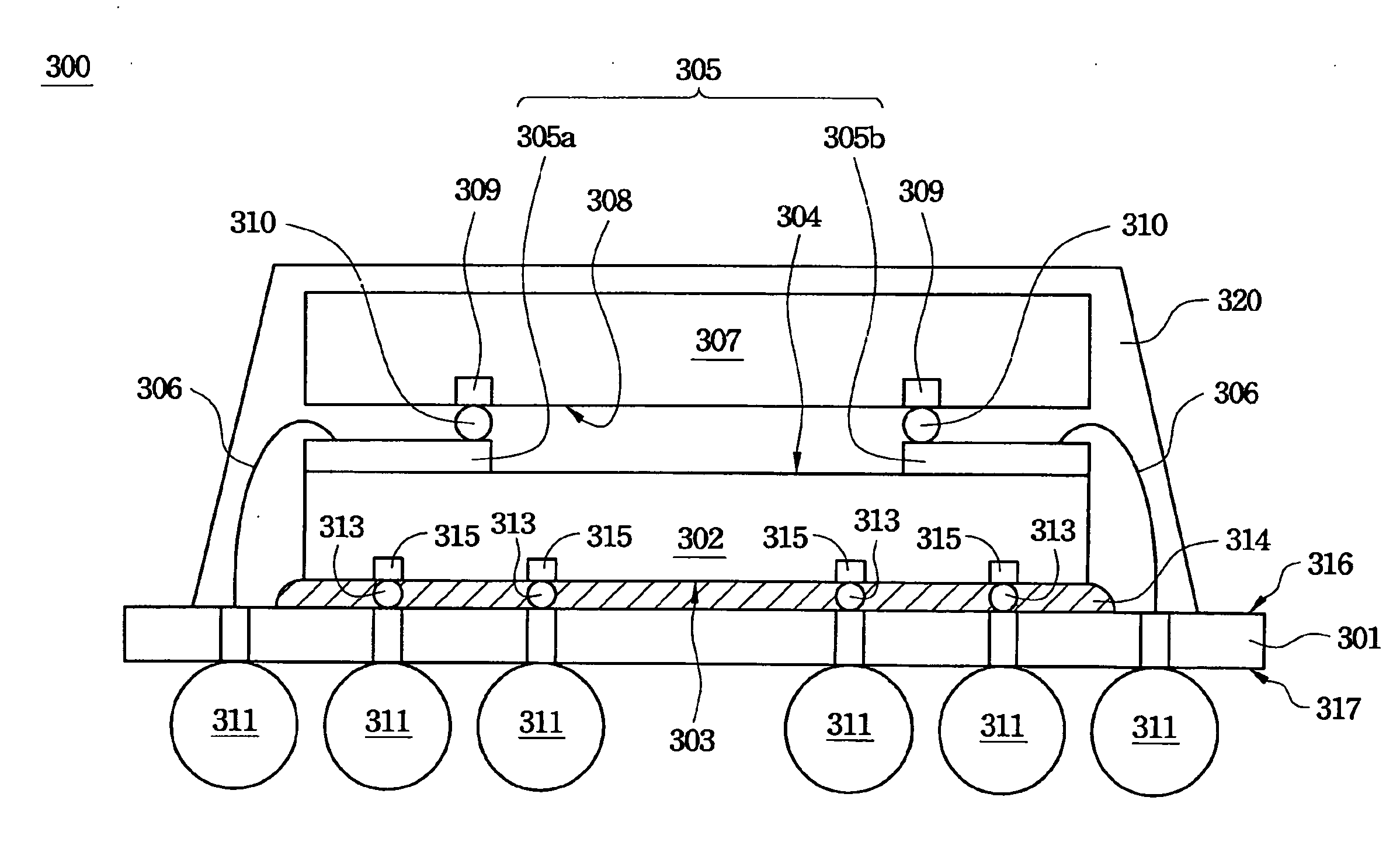
[0027]FIG. 3 illustrates a cross section view of a chip-stacked package structure 300 in accordance with a first preferred embodiment of the present invention.

[0028]The chip-stacked package structure 300 comprises a substrate 301, a first chip 302, a patterned circuit layer 305, a second chip 307 and a molding compound 320.

[0029]The chip-stacked package structure 300 is formed by the following steps: First, the substrate 301 with a first surface 316 and a second surface 317 opposite to the first surface 316 is provided. In some preferred embodiments of the present invention, the substrate 301 is a lead frame, a printed circuit board or a die carrier. In the present embodiment, the substrate 301 is a printed circuit board made of FR4 or BT epo...


PUM


Abstract

A chip stacked package structure and applications are provided, wherein the chip stacked package structure comprises a substrate, a first chip, a patterned circuit layer and a second chip. The substrate has a first surface and an opposite second surface. The first chip with a first active area and an opposite first rear surface is electrically connected to first surface of substrate by a flip chip bonding process. The patterned circuit layer set on the dielectric layer is electrically connected to the substrate via a bonding wire. The second chip set on the patterned circuit layer has a second active area and a plurality of second pads formed on the second active area, wherein the second bonding pad is electrically connected to the patterned circuit layer.

Description

RELATED APPLICATIONS[0001]The present application is based on, and claims priorities from, Taiwan Application Serial Number 96115393, filed Apr. 30, 2007, and Taiwan Application Serial Number 96117272, filed May 15, 2007, the disclosures of which are hereby incorporated by reference herein in their entirety.FIELD OF THE INVENTION[0002]The present invention relates to a semiconductor package structure and the applications thereof, and more particularly relates to a chip-stacked package structure and the applications thereof.BACKGROUND OF THE INVENTION[0003]Nowadays, electronic devices are developed to provide increased functionality. Single chips with multiple integrated functions are therefore required to have extended functionality and be able to fit into small electronic devices. To integrate more functions in a single package, the package structure of the chip has evolved from a two-dimensions to three-dimensions and from a single-die package structure to a multiple-die package s...

Claims


Application Information

Patent Timeline
Patent Type & Authority Applications(United States)
IPC IPC(8): H01L23/49
CPCH01L23/3121H01L25/0657H01L2224/04073H01L2224/16145H01L2224/32145H01L2224/48091H01L2224/48227H01L2224/48235H01L2224/4824H01L2224/4918H01L2224/731H01L2224/73265H01L2224/83102H01L2224/92125H01L2225/0651H01L2225/06513H01L2225/06517H01L2225/06527H01L2225/06582H01L2225/06589H01L2924/15311H01L2224/73215H01L24/73H01L2224/32225H01L2224/73204H01L2224/0401H01L2224/16235H01L2224/06135H01L2224/06136H01L2924/00014H01L2924/00H01L2924/00012H01L2224/023H01L2924/181H01L2224/16225H01L2924/0001
Inventor LIN, CHUN-YINGPAN, YU-TANGCHOU, SHIH-WENSHEN, GENG-SHIN
Owner CHIPMOS TECH INC
Why Eureka
Try Eureka