Chip-Stacked Package Structure and Applications Thereof

Inactive Publication Date: 2008-10-30
CHIPMOS TECH INC
View PDF5 Cites 19 Cited by
  • Summary
  • Abstract
  • Description
  • Claims
  • Application Information

AI Technical Summary

Benefits of technology

[0011]In accordance with above descriptions, the features of the present invention provide a patterned circuit layer set on a rear surface of a lower chip in a chip-stacked package structure, wherein the patterned circuit layer has at least one finger electrically connected to at least one bonding pad set on the upper chip that is stacked thereon, whereby the wiring arrangements of the second chip constituted by the bonding pad can be redistributed by the finger of the patterned circuit layer to shift the bo

Problems solved by technology

Thus the design flexibility and the number of chips stacked in a single package are limited.
Consequently, when a subsequent stamping process is conducted, the bonding wires may be wrenched off so as to make

Method used


Image

  • Chip-Stacked Package Structure and Applications Thereof
  • Chip-Stacked Package Structure and Applications Thereof
  • Chip-Stacked Package Structure and Applications Thereof

Examples


Embodiment Construction

[0018]The foregoing aspects and many of the attendant advantages of this invention will become more readily appreciated as the same becomes better understood by reference to the following preferred embodiments of chip-stacked package structures.

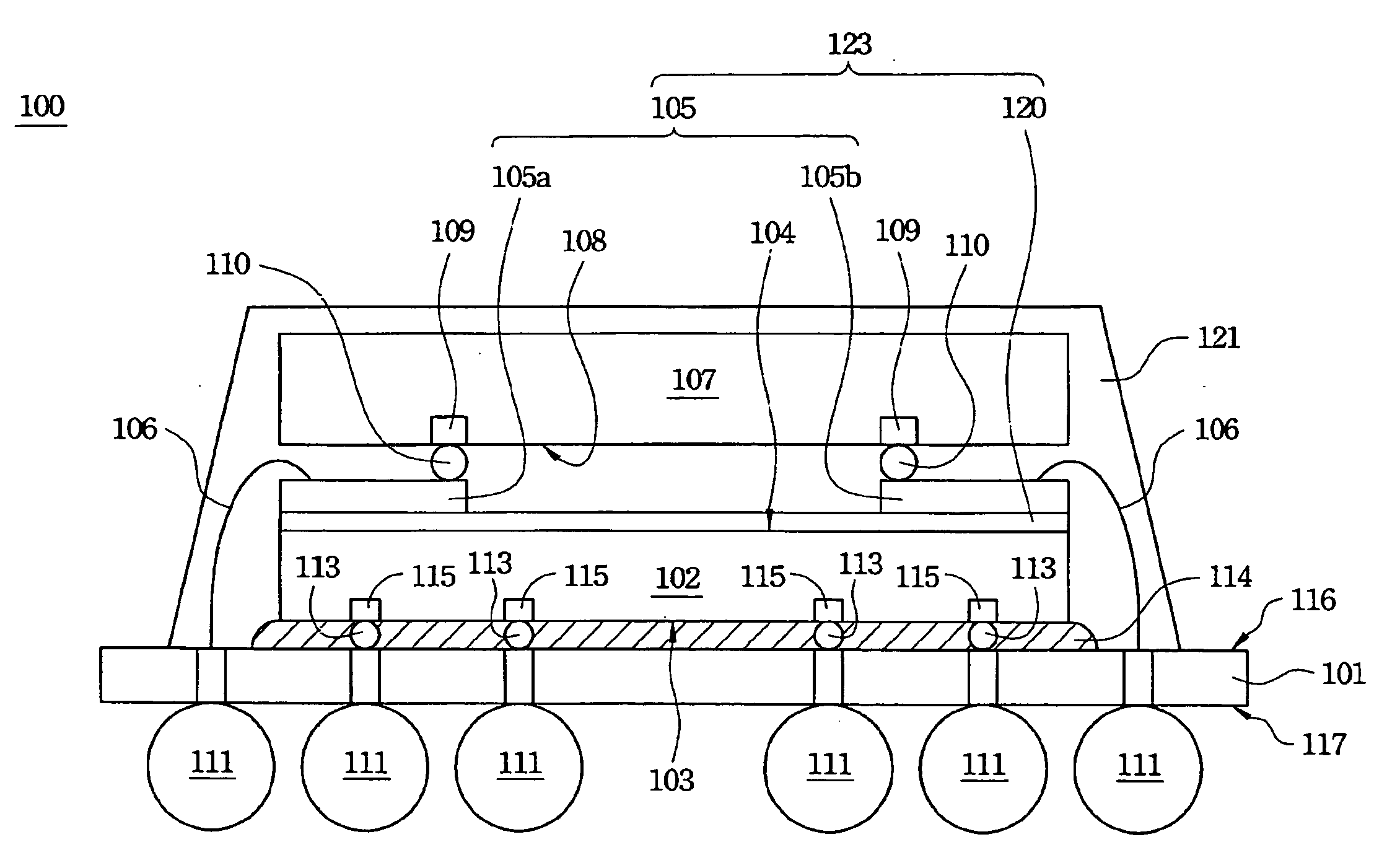
[0019]FIG. 1 illustrates a cross section view of a chip-stacked package structure 100 in accordance with a first preferred embodiment of the present invention.

[0020]The chip-stacked package structure 100 comprises a substrate 101, a first chip 102, a circuit board 123, a second chip 107 and a molding compound 120.

[0021]The chip-stacked package structure 100 is formed by the following steps: First, the substrate 101 having a first surface 116 and a second surface 117 opposite to the first surface 116 is provided. In some preferred embodiments of the present invention, the substrate 101 can be a lead frame, a printed circuit board or a die carrier. In the present embodiment, the substrate 101 is a printed circuit board made of FR4 or BT epoxy, ...


PUM


Abstract

A chip stacked package structure and applications are provided, wherein the chip stacked package structure comprises a substrate, a first chip, circuit board and a second chip. The substrate has a first surface and an opposite second surface. The first chip having a first active surface and an opposite first rear surface is electrically connected to first surface of substrate serving by a flip chip bonding process. The circuit board has a dielectric layer set on the first rear surface and a patterned conductive layer set on the dielectric layer is electrically connected to the substrate via a bonding wire. The second chip set on the patterned conductive layer has a plurality of second pads formed on a second active surface thereof and eclectically connected to the patterned conductive layer.

Description

RELATED APPLICATIONS[0001]The present application is based on, and claims priority from, Taiwan Application Serial Number 96115395, filed at Apr. 30, 2007, the disclosure of which is hereby incorporated by reference herein in its entirety.FIELD OF THE INVENTION[0002]The present invention relates to a semiconductor package structure and the applications thereof, and more particularly relates to a chip stacked package structure and the applications thereof.BACKGROUND OF THE INVENTION[0003]Nowadays, electronic devices are developed to provide increased functionality. Single chips with multiple integrated functions are therefore required to ensure and the chips can fit into electronic devices of limited. To integrate more functions in a single package, the package structure of the chip has evolved from a two-dimensions to three-dimensions and from a single-die package structure to a multiple-die package structure.[0004]A system-in-package is a chip-stacked package structure with several...

Claims


Application Information

Patent Timeline
IPC IPC(8): H01L23/04H01L21/00
CPCH01L23/3128H01L2224/06136H01L2224/16H01L2224/48091H01L2224/4824H01L2225/0651H01L2225/06513H01L2924/15311H01L25/0657H01L2224/06135H01L2224/0401H01L2224/73265H01L2224/73204H01L2224/32225H01L2224/32145H01L2224/73215H01L2924/19107H01L2224/16225H01L2924/00014H01L2924/00012H01L2224/48227H01L2924/00H01L24/73
Inventor PAN, YU-TANGCHOU, SHIH-WENLIN, CHUN-YING
Owner CHIPMOS TECH INC
Why Eureka
Try Eureka