Supercharge Your Innovation With Domain-Expert AI Agents!

Active pixel sensor and method for making same

a technology of active pixel and sensor, which is applied in the field of active pixel sensor, can solve the problem of more difficult to reduce the size of the sensing elemen

Active Publication Date: 2010-08-19
AU OPTRONICS CORP
View PDF18 Cites 10 Cited by
  • Summary
  • Abstract
  • Description
  • Claims
  • Application Information

AI Technical Summary

Benefits of technology

"The present invention provides a touch panel with a plurality of active pixel sensors arranged in an array to sense a touch event. Each sensor element includes a photo-sensing element connected to a single amplifier. The sensor element is designed to provide a sensing voltage indicative of a light level received by the photo-sensor in a sensing period. The sensing voltage is amplified by the amplifier and then reset to a predetermined voltage level in a reset period. The sensor element is designed to have a sensing voltage that is higher than the predetermined voltage level during the sensing period and lower than the predetermined voltage level during the reset period. The invention also provides a method of touch sensing and an integrated touch panel where the touch sensing elements are provided on a display panel."

Problems solved by technology

The main disadvantage of an APS over a PPS is that each of the sensing elements in the APS has more electronic components, rendering it more difficult to reduce the size of the sensing elements.

Method used


Image

  • Active pixel sensor and method for making same
  • Active pixel sensor and method for making same
  • Active pixel sensor and method for making same

Examples


Embodiment Construction

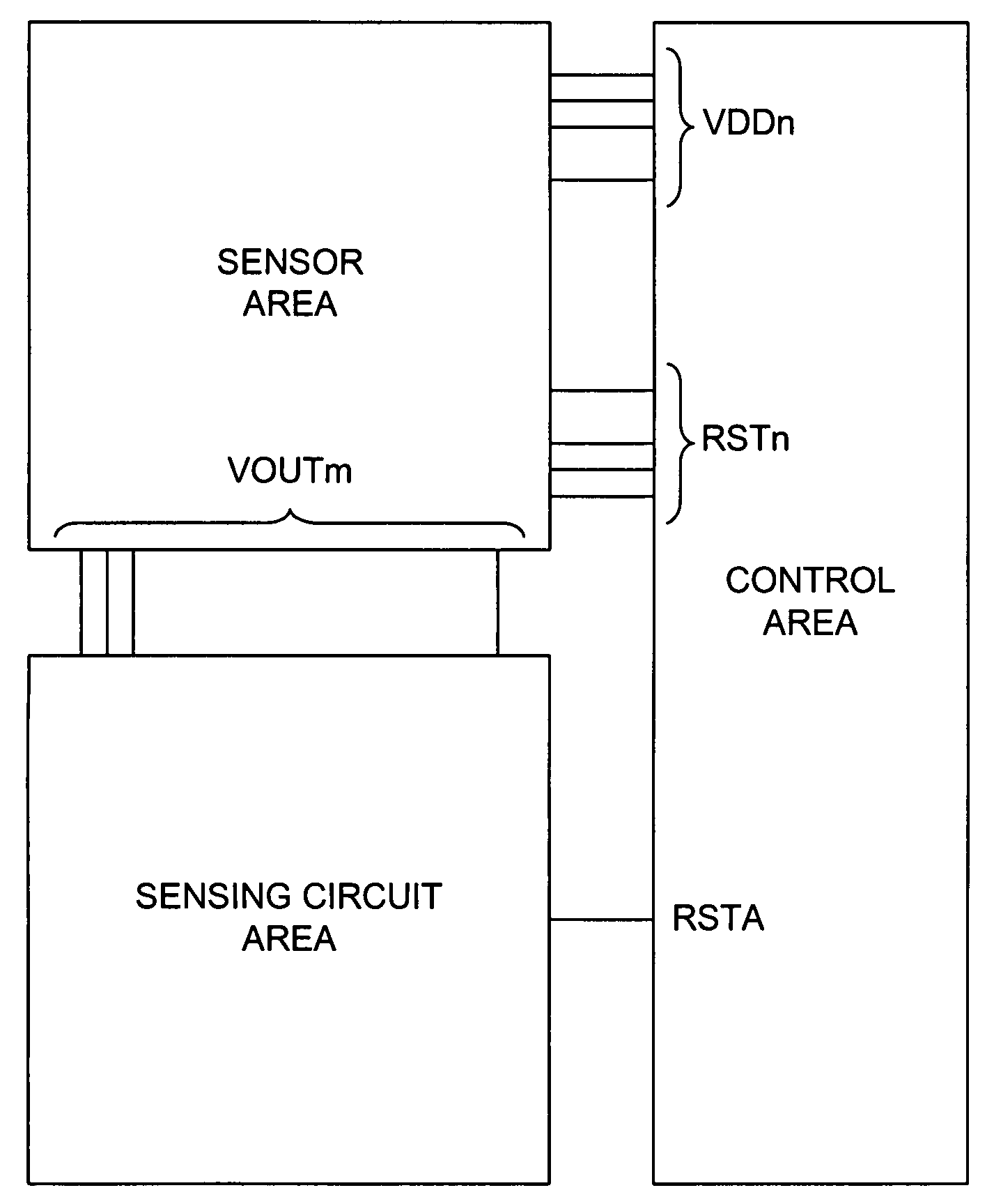
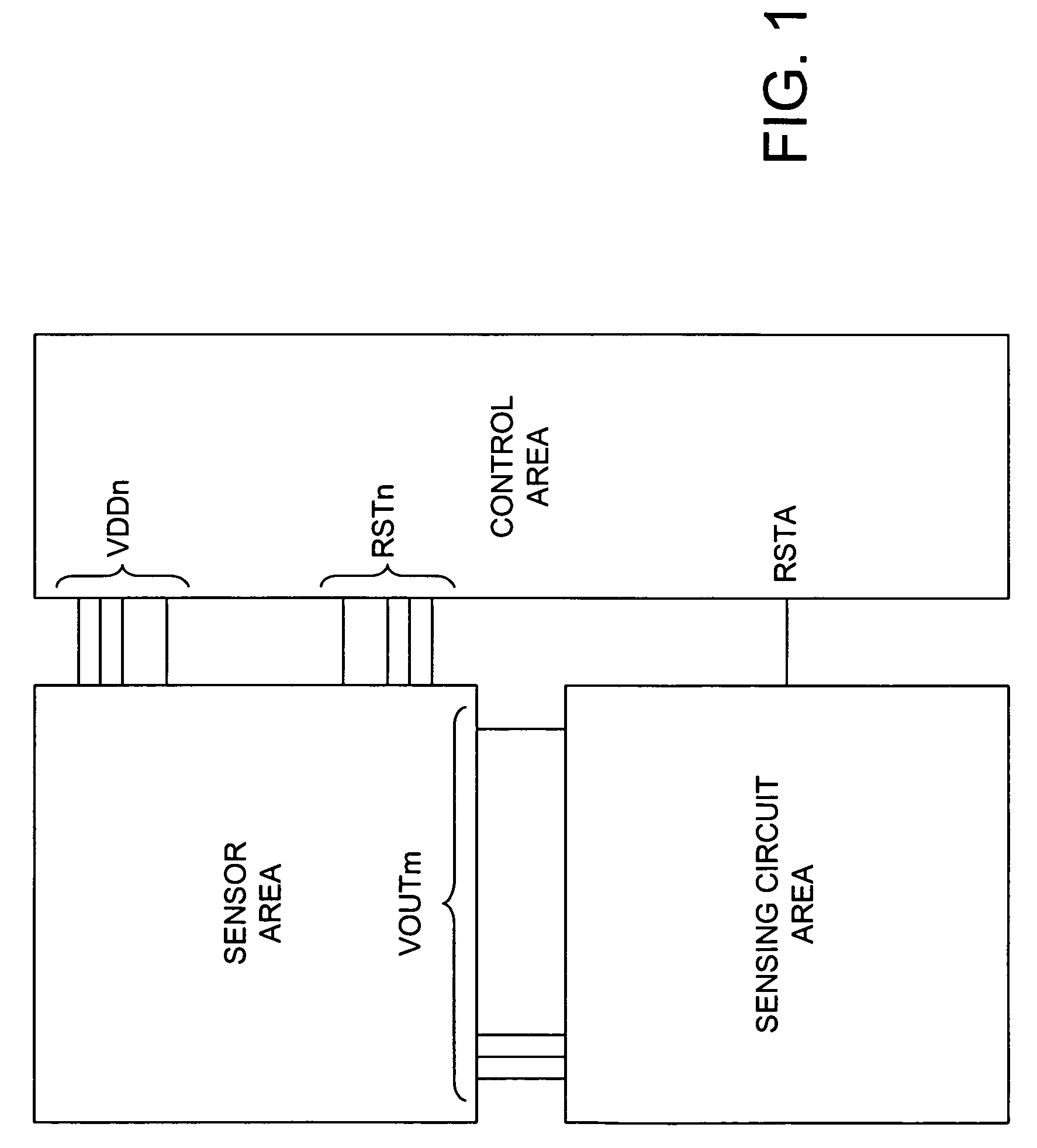
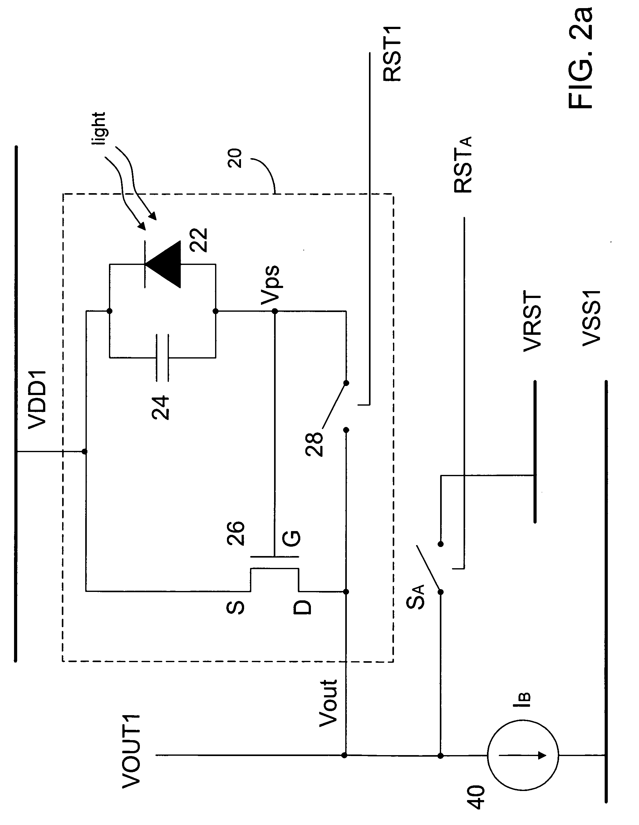
[0025]An active pixel sensor, according to embodiments of the present invention, can be divided into three areas: a sensor area, a sensing circuit area and a control area, as illustrated in FIG. 1. The sensor area comprises an array of sensor elements (see FIG. 3) to detect the light distribution on a touch screen. The sensed signals from the sensor array are transferred to the sensing circuit area for processing. The control area can be used to control the transfer of the sensed signals from the sensor array to the sensing circuit area, to reset the sensing elements, and to control the supply voltage to the sensing elements, for example. The sensor area, the sensing circuit area and the control area can be fabricated on a single substrate as an integrated circuit. At least part or all of the integrated circuit can be fabricated with low temperature poly-silicon (LTPS) on a glass substrate, for example. However, the active pixel sensor can be fabricated with other materials and on a...


PUM


Abstract

A touch panel includes a plurality of active pixel sensors arranged in an array to sense a touch event. Each sensor element includes a photo-sensing element coupled to a single amplifier. The sensor element is arranged to provide a sensing voltage indicative of a light level received by the photo-sensor in a sensing period. The sensing voltage is amplified by the amplifier into an output voltage in the sensing period. Following the sensing period, the output voltage and the sensing voltage are reset to a predetermined voltage level. Following the reset period, the photo-sensor as well as the amplifier is disabled for a period so that the sensing level is caused to drop below the predetermined voltage level.

Description

FIELD OF THE INVENTION[0001]The present invention relates generally to touch sensor array and, more particularly, to an active pixel sensor.BACKGROUND OF THE INVENTION[0002]As low temperature poly-silicon (LTPS) technology becomes mature, it would be advantageous to fabricate touch sensors along with driving circuits on a glass substrate using LTPS technology. As the term suggests, an APS is different from a passive pixel sensor (PPS) in that a sensor element in an APS has an active amplifier, such as a thin-film transistor (TFT) to amplify the sensed signal by a photo-sensor. As a result, the signal-to-noise ratio in an APS is significantly increased. The main disadvantage of an APS over a PPS is that each of the sensing elements in the APS has more electronic components, rendering it more difficult to reduce the size of the sensing elements.[0003]It is thus advantageous to provide a method for producing an APS wherein in the number of electronic components in a sensor element is r...

Claims


Application Information

Patent Timeline
Patent Type & Authority Applications(United States)
IPC IPC(8): G06F3/041H04N25/00
CPCG02F1/13338G02F2001/13312G06F3/042G06F3/0412G02F1/13312
Inventor CHEN, CHUNG-CHUNLI, YU-HSUAN
Owner AU OPTRONICS CORP
Features
  • R&D
  • Intellectual Property
  • Life Sciences
  • Materials
  • Tech Scout
  • Unparalleled Data Quality
  • Higher Quality Content
  • 60% Fewer Hallucinations
Learn More