Liquid crystal display device, electronic device comprising same, and controller for liquid crystal display device
Active Publication Date: 2010-09-23
NEC LCD TECH CORP
6 Cites 7 Cited by
AI-Extracted Technical Summary
Problems solved by technology
For this reason, this liquid crystal display suffers from lower visibility in bright places.
Consequentl...
View moreMethod used
[0107]As described above, in the display mode of the liquid crystal display, transmission sub-pixel 254 is placed into the image display state, while mirror sub-pixel 255 is placed into the non-mirror state, thereby allowing only the light that is transmitted by transmission sub-pixel 254 to exit from the front surface of liquid crystal panel 200, but not allowing the reflected light from mirror sub-pixel 255 to exit. Consequently, this liquid crystal display device can ensure high visibility of image in the display mode, even if it is used in a bright environment, because the image is not degraded in contrast due to the reflected light from mirror sub-pixel 255.
[0112]As described above, this liquid crystal display device can be switched between the display mode and the mirror mode, and can also ensure a high image quality in the display mode.
[0115]In contrast, since back light 213 can be kept ON both in the display mode and mirror mode in the liquid crystal display device according to this embodiment, the liquid crystal display device can realize a screen mode for mixing the display mode and mirror mode on a single screen by setting a first area within the screen to the display mode and by setting a second area different from the first area within the same screen to the mirror mode, in addition to a screen mode which sets the entire screen to the display mode and a screen mode whi...
View moreBenefits of technology
[0029]It is an object of the present invention to provide a liquid crystal display device which is capable of switching between a display mode and a mirror mod...
View moreAbstract
A liquid crystal display device provided herein can be switched between a display mode and a mirror mode, and can ensure a high image quality in the display mode.
The liquid crystal display device comprises liquid crystal panel 200 including sub-pixels 254, 255, and back light 213 for irradiating light to the back surface of liquid crystal panel 200. Transmission sub-pixel 254 can be switched into an image display state which can allow irradiated light to exit, and a black display state which does not allow irradiated light to exit. Mirror sub-pixel 255 can be switched between a mirror state which can allow reflected light to exit and a non-mirror state which does not allow reflected light to exit, independently of transmission sub-pixel 254. A control unit places each transmission sub-pixel 254 into the image display state or black display state, and places each mirror sub-pixel 255 into the mirror state or non-mirror state.
Application Domain
Technology Topic
Image
Examples
- Experimental program(11)
Example
First Embodiment
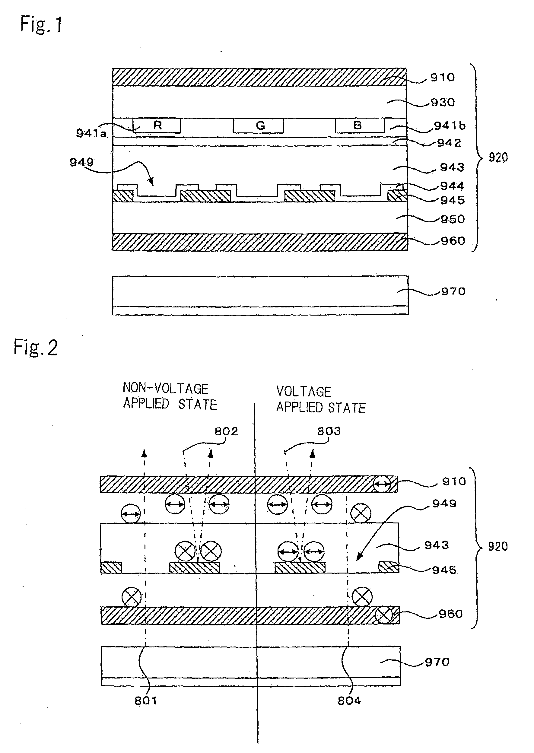
[0085]FIG. 5 is a schematic diagram showing the configuration of circuits in a liquid crystal display device according to a first embodiment of the present invention. This liquid crystal display device comprises two types of sub-pixels: transmission sub-pixels 254 which is a transmission area that allows light irradiated from a back light to be transmitted, and mirror sub-pixel 255 which is a mirror area that reflects external light to produce a mirror state. In this liquid crystal display device, one pixel is made up of a plurality of transmission sub-pixels 254 and a plurality of mirror sub-pixels 255.
[0086]The liquid crystal display device according to this embodiment is characterized in that each transmission sub-pixel 254 and each mirror sub-pixel 255 can be controlled independently, as will be later described in detail. In this way, this liquid crystal display device can realize a screen mode in which a display mode and a mirror mode can be mixed on a single screen.
[0087]In this embodiment, each transmission sub-pixel 254 and each mirror sub-pixel 255 are controlled independently in an active matrix scheme. The active matrix scheme refers to a scheme for controlling the driving of each sub-pixel using a switching element such as a thin-film transistor (TFT) included in each sub-pixel.
[0088]Transmission sub-pixels 254 and mirror sub-pixels 255 are arrayed to form a plurality of rows, each of which comprises one of transmission sub-pixels 254 and mirror sub-pixels 255 arranged in a line in the horizontal direction, where rows of transmission sub-pixels 254 and mirror sub-pixels 255 alternate with each other in the array. Accordingly, when the sub-pixels of the liquid crystal display device are viewed as columns in the vertical direction, rather than as rows in the horizontal direction, transmission sub-pixels 254 and mirror sub-pixels 255 alternate with each other.
[0089]Each transmission sub-pixel 254 is provided with transmission sub-pixel electrode 211, while each mirror sub-pixel 255 is provided with mirror sub-pixel electrode 212.
[0090]This liquid crystal display device is provided with drain line 252 which is a signal line extending in the vertical direction along each column of the sub-pixels. Here, Dn designates drain line 252 which corresponds to a sub-pixel on an n-th column. Specifically, drains lines 252 corresponding to sub-pixels on the first column, second column, third column, and fourth column from the left in FIG. 5 are designated by D1, D2, D3, and D4, respectively.
[0091]Also, this liquid crystal display device is provided with gate line 253 which is a scan line extending in the horizontal direction along each row of the sub-pixels. Here, Gn designates gate line 253 corresponding to a sub-pixel on an n-th row. Specifically, gate lines 253 corresponding to sub-pixels on the first row, second row, third row, and fourth row from the top in FIG. 5 are designated by G1, G2, G3, and G4, respectively.
[0092]Each of transmission sub-pixel 254 and mirror sub-pixel 255 is individually provided with TFT 251 near the intersection of drain line 252 with gate line 253, and TFT 251 is connected to sub-pixel electrode 211, 212, respectively, provided in each sub-pixel. TFT 251 is also connected to drain line 252 and gate line 253 corresponding to each sub-pixel 254, 255. Each TFT 251 is controlled by a signal supplied to gate line 253 connected thereto.
[0093]In this way, each sub-pixel 254, 255 can be controlled through drain line 252 and gate line 253 corresponding thereto in an active matrix scheme. Specifically, transmission sub-pixel 254 appearing at the upper leftmost corner in FIG. 5, for example, is controlled through drain line D1 and gate line G1, and mirror sub-pixel 255 immediately below transmission sub-pixel 254 is controlled through drain line D1 and gate line G2.
[0094]FIG. 6 is a cross-sectional view of the liquid crystal display device shown in FIG. 5, taken along line A-A′. Specifically, FIG. 6 shows sub-pixels on the first column of the liquid crystal display device in FIG. 5. As can be seen, gate line 253 is omitted in FIG. 6. This liquid crystal display device comprises liquid crystal panel 200 for displaying an image, and back light 213 which is a light source for irradiating liquid crystal panel 200 with light from below, as viewed in FIG. 6. Here, the top surface of liquid crystal panel 200 is defined as a front surface, and the bottom surface of the liquid crystal panel 200 is defined as a back surface. This liquid crystal display device permits the user to observe liquid crystal panel 200 as a screen from the front surface side of liquid crystal panel 200.
[0095]Liquid crystal panel 200 comprises upper substrate 203 and lower substrate 207 arranged in opposition to each other. λ/4 plate 202 is disposed on the top surface of upper substrate 203, and polarizer plate 201 is disposed on the top surface of λ/4 plate 202. Similarly, λ/4 plate 208 is disposed on the bottom surface of lower substrate 207, and polarizer plate 209 is disposed on the bottom surface of λ/4 plate 208.
[0096]Coloring layer 210 covered with protection film 204 is disposed on the bottom surface of upper substrate 203, and common electrode 205 is disposed on a bottom surface of protection film 204. Also, transmission sub-pixel electrodes 211 and mirror sub-pixel electrodes 212 are alternately disposed on the top surface of lower substrate 207. Mirror sub-pixel electrode 212 is formed of a material which exhibits a high reflectivity such that its top surface is even, and therefore functions not only as an electrode but also as a reflection member for reflecting external light incident thereon from above.
[0097]Liquid crystal layer 206 is also disposed between upper substrate 203 and lower substrate 207. Liquid crystal layer 206 is filled with liquid crystal which is aligned in a direction perpendicular to the surfaces of the respective substrates. Voltage can be individually applied between each sub-pixel electrode 211, 212 and common electrode 205, so that liquid crystal layer 206 can be applied with different voltages for each sub-pixel 254, 255.
[0098]This liquid crystal display device employs a display scheme called “VA scheme.” Liquid crystal layer 206 is such that liquid crystal molecules align in the direction perpendicular to substrates 203, 207 in a non-voltage applied state where no voltage is applied between sub-pixel electrode 211, 212 and common electrode 205, to give no phase difference to light which is transmitted through liquid crystal layer 206 in the thickness direction. On the other hand, in a voltage applied state where a predetermined voltage is applied between common electrode 205 and sub-pixel electrode 211, 212, liquid crystal layer 206 is such that liquid crystal molecules align in a direction inclined from the direction perpendicular to substrates 203, 207, giving a predetermined phase difference to light which is transmitted through liquid crystal layer 206 in the thickness direction.
[0099]Coloring layer 210 is disposed at a position opposite to transmission sub-pixel electrode 211. Accordingly, as light is transmitted through transmission sub-pixel electrode 211 and is transmitted through coloring layer 210, the light is colored in a color according to coloring layer 210. Transmission sub-pixels 254 comprise those for displaying red, those for displaying green, and those for displaying blue, and coloring layer 210 used in each transmission sub-pixel 254 corresponds to a color to be displayed.
[0100]In FIG. 5, “R” represents transmission sub-pixel 254 for displaying red; “G” represents transmission sub-pixel 254 for displaying green; and “B” represents transmission sub-pixel 254 for displaying blue. As shown in FIG. 5, colors displayed by transmission sub-pixels 254 are red on the first column, green on the second column, and blue on the third column, and are arranged in the order of red, green, and blue on the fourth column onward. As can be seen, mirror sub-pixels 255 are all labeled “M” in FIG. 5.
[0101]In this liquid crystal display device, one pixel is made up of six sub-pixels indicated by a broken line which surrounds them in FIG. 5. Specifically, one pixel includes transmission sub-pixels 254 each for displaying red, blue, and green, and three mirror sub-pixels 255.
[0102]FIG. 7A is a diagram indicating trajectories of light in the display mode of the liquid crystal display device. Polarizer plate 201 and polarizer plate 209 are disposed such that their polarization transmission axes are orthogonal to each other. Specifically, polarizer plate 201 exhibits a polarization transmission axis in a direction parallel to the drawing sheet of FIG. 7A as indicated by circled arrows in FIG. 7A, while polarizer plate 209 exhibits a polarization transmission axis in a direction perpendicular to the drawing sheet as indicated by a circled mark “X.”
[0103]In transmission sub-pixel 254 in the display mode, the absolute value of voltage applied to liquid crystal layer 206 should be chosen to be equal to or higher than a voltage value at which transmission sub-pixel 254 enters a non-voltage applied state, i.e., 0 V or higher, and equal to or lower than a voltage value at which light is maximally emitted. Also, in mirror sub-pixel 254 in the display mode, no voltage is applied to liquid crystal layer 206, so that mirror sub-pixel 254 remains in the non-voltage applied state.
[0104]FIG. 7A shows, by way of example, that transmission sub-pixel 254 is in a voltage applied state. In his voltage applied state of the liquid crystal display device in the display mode, voltage applied between common electrode 205 and transmission sub-pixel electrode 211 is set such that light transmitting liquid crystal layer 206 is given a phase difference of λ/2.
[0105]In the display mode of the liquid crystal display device, arrow 222 indicates a trajectory of light irradiate from back light 213 to transmission sub-pixel 254 in the voltage applied state, and arrow 223 indicates a trajectory of external light incident on mirror sub-pixel 255 in the non-voltage applied state. In this way, polarizer plate 201 is transmitted by the light irradiated from back light 213 to transmission sub-pixel 254 in the voltage applied state, but is not transmitted by the external light incident on mirror sub-pixel 255 in the non-voltage applied state and is reflected by mirror sub-pixel electrode 212.
[0106]Accordingly, in the display mode of the liquid crystal display device, transmission sub-pixel 254 is placed into an image display state where the irradiated light incident on transmission sub-pixel 254 can be allowed to exit from the front surface of liquid crystal panel 200, while mirror sub-pixel 254 is placed into a non-mirror state where the external light reflected by mirror sub-pixel electrode 212 is not allowed to exit from the front surface of liquid crystal panel 200.
[0107]As described above, in the display mode of the liquid crystal display, transmission sub-pixel 254 is placed into the image display state, while mirror sub-pixel 255 is placed into the non-mirror state, thereby allowing only the light that is transmitted by transmission sub-pixel 254 to exit from the front surface of liquid crystal panel 200, but not allowing the reflected light from mirror sub-pixel 255 to exit. Consequently, this liquid crystal display device can ensure high visibility of image in the display mode, even if it is used in a bright environment, because the image is not degraded in contrast due to the reflected light from mirror sub-pixel 255.
[0108]FIG. 7B is a diagram showing trajectories of light in the mirror mode of the liquid crystal display device. In the mirror mode of the liquid crystal display device, transmission sub-pixel 254 is placed into a non-voltage applied state by applying no voltage to liquid crystal layer 206. Also, in the mirror mode, mirror sub-pixel 255 is placed into a voltage applied state by applying a predetermined voltage to liquid crystal layer 206.
[0109]In the mirror mode of the liquid crystal display device, a voltage applied between common electrode 205 and mirror sub-pixel electrode 212 in the voltage applied state is set such that light transmitting liquid crystal layer 206 is given a phase difference of λ/4.
[0110]In the mirror more of the liquid crystal display device, arrow 221 indicates a trajectory of light emitted from back light 213 to transmission sub-pixel 254 in the non-voltage applied state, and arrow 224 indicates a trajectory of external light incident on mirror sub-pixel 255 in the voltage applied state. In this way, polarizer plate 201 is not transmitted by the light irradiated from back light 213 to transmission sub-pixel 254 in the non-voltage applied state, but is transmitted by the external light incident on mirror sub-pixel 255 in the non-voltage applied state and reflected by mirror sub-pixel electrode 212.
[0111]Accordingly, in the mirror mode of the liquid crystal display device, transmission sub-pixel 254 is placed into a black display state where the irradiated light incident on transmission sub-pixel 254 is not allowed to exit from the front surface of liquid crystal panel 200, while mirror sub-pixel 255 is placed into a mirror state where the external light reflected by mirror sub-pixel electrode 212 is allowed to exit from the front surface of liquid crystal panel 200.
[0112]As described above, this liquid crystal display device can be switched between the display mode and the mirror mode, and can also ensure a high image quality in the display mode.
[0113]Notably, in this liquid crystal display device, since the light irradiated from back light 213 and incident on transmission sub-pixel 254 is not emitted from the front surface of liquid crystal panel 200 in the mirror mode, back light 213 need not be switched from ON to OFF when the liquid crystal display device is switched from the display mode to the mirror mode.
[0114]In a liquid crystal display device which involves turning a back light from ON to OFF when it is switched from the display mode to the mirror mode, as the one described in JP2004-170792A, the back light is ON in the display mode, and OFF in the mirror mode. For this reason, such a liquid crystal display device experiences difficulties in realizing a screen mode for mixing the display mode and mirror mode on a single screen, though the liquid crystal display device can provide a screen mode for setting the overall screen to the display mode and a screen mode for setting the overall screen to the mirror mode.
[0115]In contrast, since back light 213 can be kept ON both in the display mode and mirror mode in the liquid crystal display device according to this embodiment, the liquid crystal display device can realize a screen mode for mixing the display mode and mirror mode on a single screen by setting a first area within the screen to the display mode and by setting a second area different from the first area within the same screen to the mirror mode, in addition to a screen mode which sets the entire screen to the display mode and a screen mode which sets the entire screen to the mirror mode. With the realization of the screen mode for mixing the display mode and mirror mode, the liquid crystal display device can be improved as regards the degree of freedom in screen layout, leading to resulting improvements in practicability and decorativeness.
[0116]FIGS. 8A-8E are diagrams illustrating the above screen mode of the liquid crystal display device. Specifically, FIGS. 8A-8E show (1) the state of transmission sub-pixel 254, (2) the state of mirror sub-pixel 255, and (3) a screen actually observed by the user.
[0117]FIGS. 8A-8E (1) show that transmission sub-pixels 254 are in an image display state within an area in which a black character “A” is displayed on a white background, and that transmission sub-pixels 254 are in a black display state within a solid black area.
[0118]FIGS. 8A-8E (2) show that mirror sub-pixels 255 are in a mirror state within a shaded area, and that mirror sub-pixels 255 are in a non-mirror state within a solid black area.
[0119]FIGS. 8A-8E (3) show that the display mode is set to an area in which a black character “A” is shown on a white background within the screen, and that the mirror mode is set to a shaded area.
[0120]FIG. 8A shows a screen mode in which the entire screen is set to the display mode. In this screen mode, all transmission sub-pixels 254 are placed into an image display state, while all mirror sub-pixels 255 are placed into a non-mirror state.
[0121]FIG. 8B shows a screen mode in which the entire screen is set to the mirror mode. In this screen mode, all transmission sub-pixels 254 are placed into a black display state, while all mirror sub-pixels 255 are placed into a mirror state.
[0122]FIG. 8C shows a screen mode in which the display mode and mirror mode are mixed by setting the left half of the screen to the display mode and the right half of the screen to the mirror mode. In this screen mode, transmission sub-pixels 254 are placed into the image display state in the left half of the screen, while transmission sub-pixels 254 are placed into the black display state in the right half of the screen. Further, mirror sub-pixels 255 are placed into the non-mirror state in the left half of the screen, while mirror sub-pixels 255 are placed into the mirror state in the right half of the screen.
[0123]FIG. 8D shows a screen mode in which the display mode and mirror mode are mixed by setting the upper half of the screen to the display mode and the lower half of the screen to the mirror mode. In this screen mode, transmission sub-pixels 254 are placed into the image display state in the upper half of the screen, while transmission sub-pixels 254 are placed into the black display state in the lower half of the screen. Further, mirror sub-pixels 255 are placed into the non-mirror state in the upper half of the screen, while mirror sub-pixels 255 are placed into the mirror state in the lower half of the screen.
[0124]FIG. 8E shows a screen mode in which the display mode and mirror mode are mixed by setting a lower left area of the screen to the display mode and the remaining area of the screen except for the lower left area to the mirror mode. In this screen mode, transmission sub-pixels 254 are placed into the image display state in the lower left area of the screen, while transmission sub-pixels 254 are placed into the black display state in the remaining screen except for the lower left area. Further, mirror sub-pixels 255 are placed into the non-mirror state in the lower left area of the screen, while mirror sub-pixels 255 are placed into the mirror state in the remaining area of the screen except for the lower left area.
[0125]FIG. 9 is a block diagram showing a screen control function of the liquid crystal display device, and FIG. 10 shows an example of screen control process in accordance with the screen control function of FIG. 9. FIG. 10 shows a screen control process in the screen mode shown in FIG. 8E, as an example of the screen control.
[0126]This liquid crystal display device comprises control unit 401 for controlling transmission sub-pixels 254, mirror sub-pixels 255, and back light 213. Control unit 401 may be provided as a controller independent of the liquid crystal display device. Control unit 401 comprises processing control unit 411, transmission signal input unit 402, combiner unit 403, mirror signal input unit 404, combiner unit 405, combiner unit 406, and screen control unit 407. Processing control unit 411 controls the respective components based on signals applied thereto from user interface 412.
[0127]When a signal is applied to processing control unit 411 from user interface 412, processing control unit 411 first applies transmission signal input unit 402 with a transmission signal which includes image display information 301 for placing transmission sub-pixels 254 into an image display state and black display information 304 for placing transmission sub-pixels 254 into a black display state. Additionally, simultaneously with the foregoing, processing control unit 411 applies mirror signal input unit 404 with a mirror signal which includes non-mirror information 302 for placing mirror sub-pixels 255 into a non-mirror state and mirror information 305 for placing mirror sub-pixels 255 into a mirror state.
[0128]Upon receipt of the transmission signal, transmission signal input unit 402 sends image display information 301 and black display information 304 to combiner unit 403. Combiner unit 403 combines image display information 301 and black display information 304 based on a transmission position signal applied thereto from processing control unit 411 to form transmission sub-pixel information 313. Combiner 403 sends transmission sub-pixel information 313 to combiner 406.
[0129]Upon receipt of the mirror signal, mirror signal input unit 404 sends non-mirror information 302 and mirror information 305 to combiner unit 405. Combiner unit 405 combines non-mirror information 302 and mirror information 305 based on mirror position signal applied thereto from processing control unit 411 to form mirror sub-pixel information 314. Combiner unit 405 sends mirror sub-pixel information 314 to combiner 406.
[0130]Combiner 406 further combines transmission sub-pixel information 313 with mirror sub-pixel information 314 in such a manner that the base of transmission sub-pixel information 313 is bound to the upside of mirror sub-pixel information 314 to form screen control information 316. Then, combiner unit 406 sends screen control information 316 to screen control unit 407, so that screen control unit 407 drives transmission sub-pixels 254 and mirror sub-pixels 255 in accordance with screen control information 316.
[0131]Control unit 401 can conduct screen control in other screen modes in a similar manner. For example, control unit 401 sets the entire screen shown in FIG. 8A to the display mode executing control as shown in FIG. 11, and sets the screen mode for setting the entire screen to the mirror mode, as shown in FIG. 8B, by conducing control as shown in FIG. 12.
[0132]A switching between the screen modes is performed by applying a mode switching signal to user interface 412 which serves as an input unit.
[0133]Referring next to FIGS. 13A and 13B, a description will be given of how to drive sub-pixels 254, 255 of the liquid crystal display device. While this liquid crystal display device employs a gate line inversion drive, the present invention can otherwise employ, for example, a source line inversion drive, a dot inversion drive, a frame inversion drive, and the like.
[0134]Here, a Gn duration designates a duration in which a voltage is applied to Gn among gate lines 253 shown in FIG. 5 to select a sub-pixel connected to Gn. Specifically, durations in which a voltage is applied to G1, G2, G3, G4 are designated by G1 duration, G2 duration, G3 duration, and G4 duration, respectively. While FIGS. 13A and 13B show the waveforms in G1 duration, they also applied to Gn duration other than G1 duration.
[0135]Referring first to FIG. 13A, a description will be given of the display mode of the liquid crystal display device. FIG. 13A shows the waveforms of voltages VG, VD, and VCOM which are applied to gate line 253, drain line 252, and common electrode 205, respectively, during G1 duration in the display mode.
[0136]The value of VG is set to VGH only during Gn duration for selecting a sub-pixel connected to each gate line 253 (Gn) and to VGL during the remaining durations. Specifically, the value of VG is VGH only during G1 duration, and VGL during the remaining durations. The value of VD can be determined within a range of VDL or higher to VDH or lower.
[0137]VCOM presents a common waveform both in the display mode and mirror mode. VCOM takes the values of VCH and VCL which is alternated each duration, and is also alternated each frame. Specifically, in the frame shown in FIG. 13A, VCOM has the value of VCL in G1 duration and VCH in G2 duration, and in the next frame. VCOM has the value of VCH in G1 duration and VCL in G2 duration.
[0138]It is assumed in this embodiment that VDH=VCH and VDL=VCL. More specifically, VDH=6V, VDL=1V, VCH=6V, and VCL=1V.
[0139]During G1 duration in the frame shown in FIG. 13A, a voltage having the value of (VD−VCL) is applied between transmission sub-pixel electrode 211 and common electrode 205 of transmission sub-pixel 254 connected to G1. Since the value of VD is equal to or higher than VCL in any transmission sub-pixel 254, a voltage having the value of 0 V or higher should be applied between transmission sub-pixel electrode 211 and common electrode 205. Notably, transmission sub-pixel 254 is placed into a voltage applied state when the value of VD is VDH.
[0140]Accordingly, transmission sub-pixel 254 connected to G1 at this time is in an image display state because a positive voltage can be applied between transmission sub-pixel electrode 211 and common electrode 205 by adjusting the value of VD.
[0141]Also, during Gn duration in the frame shown in FIG. 13A, since the value of VD is also equal to or higher than VCL in transmission sub-pixels 254 connected to gate lines 253 (Gn) other than G1, a voltage having the value of 0 V or higher should be applied between transmission sub-pixel electrode 211 and common electrode 205. Accordingly, any of transmission sub-pixels 254 connected to Gn at this time is in an image display state.
[0142]During G1 duration in the frame next to that shown in FIG. 13A, a voltage having the value of (VD−VCH) is applied between transmission sub-pixel electrode 211 and common electrode 205 of transmission sub-pixel 254 connected to G1. Since the value of VD is equal to or lower than VCH in any of transmission sub-pixels 254, a voltage having the value of 0 V or lower should be applied between transmission sub-pixel electrode 211 and common electrode 205. Notably, transmission sub-pixel 254 is placed into a voltage applied state when the value of VD is VDL.
[0143]Accordingly, transmission sub-pixel 254 connected to G1 at this time is in an image display state because a negative voltage can be applied between transmission sub-pixel electrode 211 and common electrode 205 by adjusting the value of VD.
[0144]Also, during Gn duration in the frame next to that shown in FIG. 13A, since the value of VD is also equal to or lower than VCH in transmission sub-pixels 254 connected to gate lines 253 (Gn) other than G1 during Gn duration, a voltage having the value of 0 V or lower should be applied between transmission sub-pixel electrode 211 and common electrode 205. Accordingly, any of transmission sub-pixels 254 connected to Gn at this time remains in an image display state.
[0145]As described above, this liquid crystal display device employs the gate line inversion drive. But when only transmission sub-pixel 254 in the display mode is focused on, the liquid crystal display device is driven in a manner similar to a frame inversion driving method because the polarity of the voltage applied between transmission sub-pixel electrode 211 and common electrode 205 is inverted for every frame but is not inverted for every gate line 253.
[0146]Also, during Gn duration in the display mode of this liquid crystal display device, the value of VD is set equal to the value of VCOM in any of mirror sub-pixels 255 connected to Gn. In this way, a voltage having the value of 0 V is applied between mirror sub-pixel electrode 212 and common electrode 205 in any mirror sub-pixel 255, so that mirror sub-pixel 255 is placed into a non-voltage applied state and accordingly is placed in a non-mirror state.
[0147]This liquid crystal display device can place transmission sub-pixels 254 into an image display state and place mirror sub-pixels 255 into a non-mirror state by driving sub-pixels 254, 255 in the foregoing manner. In this way, this liquid crystal display device can realize the display mode.
[0148]Referring next to FIG. 13B, a description will be given of the mirror mode of the liquid crystal display device. FIG. 13B shows the waveforms of voltages VG, VD, and VCOM applied to gate line 253, drain line 252, and common electrode 205, respectively, during G1 duration in the mirror mode.
[0149]The value of VG is set to VGH only during Gn duration for selecting a sub-pixel connected to each gate line 253 (Gn) and to VGL during the remaining durations. Specifically, the value of VG at G1 is VGH only during G1 duration, and VGL during the remaining durations.
[0150]VD takes the values of VDH and VDL which are alternated every frame. Specifically, the value of VD is VDL in a frame shown in FIG. 13B, and the value of VD is VDH in the next frame. Notably, in this embodiment, since a phase difference of λ/4 must be given to light which is transmitted liquid crystal layer 206 in mirror sub-pixel 255 in a voltage applied state, the value of VD is set to VD1 lower than VDH or to VD2 higher than VDL during a period (G2 duration, G4 duration, . . . ) for selecting gate electrode 253 connected to mirror sub-pixel 255. In this embodiment, VD1=4V, and VD2=3V.
[0151]During G1 duration in the frame shown in FIG. 13B, a voltage having the value of (VD−VCL) is applied between transmission sub-pixel electrode 211 and common electrode 205 of transmission sub-pixel 254 connected to G1. Since the value of VD is VDL in any of transmission sub-pixels 254, a voltage having the value of 0 V is applied between transmission sub-pixel electrode 211 and common electrode 205. Accordingly, since any one of transmission sub-pixels 254 connected to G1 at this time is placed into a non-voltage applied state, this one sub-pixel presents a black display state.
[0152]Also, during Gn duration in the frame shown in FIG. 13B, since the value of VD is also equal to VDL in transmission sub-pixels 254 connected to gate lines 253 (Gn) other than G1 during Gn duration, a voltage having the value of 0 V or lower should be applied between transmission sub-pixel electrode 211 and common electrode 205. Accordingly, since any one of transmission sub-pixels 254 connected to Gn at this time is placed into a non-voltage applied state, this one sub-pixel presents a black display state.
[0153]During G1 duration in the frame next to that shown in FIG. 13B, a voltage having the value of (VD−VCH) is applied between transmission sub-pixel electrode 211 and common electrode 205 of transmission sub-pixel 254 connected to G1. Since the value of VD is equal to VDH in any of transmission sub-pixels 254, a voltage having the value of 0 V should be applied between transmission sub-pixel electrode 211 and common electrode 205. Accordingly, since any one of transmission sub-pixels 254 connected to G1 at this time is placed into a non-voltage applied state, this one sub-pixel presents a black display state.
[0154]Also, during Gn duration in the frame next to that shown in FIG. 13B, since the value of VD is also equal to VDH in transmission sub-pixels 254 connected to gate lines 253 (Gn) other than G1 during Gn duration, a voltage having the value of 0 V should be applied between transmission sub-pixel electrode 211 and common electrode 205. Accordingly, since any one of transmission sub-pixels 254 connected to Gn at this time is placed into a non-voltage applied state, this one sub-pixel presents a black display state.
[0155]During G2 duration in the frame shown in FIG. 13B, a voltage having the value of (VD−VCH) is applied between mirror sub-pixel electrode 212 and common electrode 205 of mirror sub-pixel 255 connected to G2. Since the value of VD is equal to VD2 in any of mirror sub-pixels 255, a voltage having the value of (VD2−VCH) is applied between mirror sub-pixel electrode 212 and common electrode 205. In this event, since any one of mirror sub-pixels 255 is placed into a voltage applied state, this one sub-pixel presents a mirror state.
[0156]Also, during Gn duration in the frame shown in FIG. 13B, the value of VD is also equal to VD2 in mirror sub-pixels 255 connected to gate lines 253 (Gn) other than G2 during Gn duration. Since any one of mirror sub-pixels 255 is placed into a voltage applied state, this one sub-pixel presents a mirror state.
[0157]During G2 duration in the frame next to that shown in FIG. 13B, a voltage having the value of (VD−VCL) is applied between mirror sub-pixel electrode 212 and common electrode 205 of mirror sub-pixel 255 connected to G2. Since the value of VD is equal to VD1 in any of mirror sub-pixels 255, a voltage having the value of (VD1−VCL) is applied between mirror sub-pixel electrode 212 and common electrode 205. In this event, since any one of mirror sub-pixels 255 is placed into a voltage applied state, this one sub-pixel presents a mirror state.
[0158]Also, during G2 duration in the frame next to that shown in FIG. 13B, the value of VD is also equal to VD1 during Gn duration in mirror sub-pixels 255 connected to gate lines 253 (Gn) other than G2. Since any one of mirror sub-pixels 255 is placed into a voltage applied state, this one sub-pixel presents a mirror state.
[0159]As described above, this liquid crystal display device employs the gate line inversion driving method. But when only on mirror sub-pixel 255 in the mirror mode is focused on, the liquid crystal display device is driven in a manner similar to a frame inversion driving method because the polarity of the voltage applied between mirror sub-pixel electrode 212 and common electrode 205 is inverted for every frame but is not inverted for every gate line 253.
[0160]This liquid crystal display device can place transmission sub-pixels 254 into a black display state as well as place mirror sub-pixels 255 into a mirror state by driving sub-pixels 254, 255 in the foregoing manner. In this way, this liquid crystal display device can realize the mirror mode.
[0161]FIG. 14 is a perspective view of an electronic device to which the liquid crystal display device according to this embodiment can be applied. While FIG. 14 shows a portable telephone as one example of electronic device 501, the liquid crystal display device according to this embodiment can also be applied to a variety of portable terminal devices except for the portable telephone, such as portable information terminals (PDA: Personal Digital Assistants), game machines, digital cameras, digital video cameras and so on. Further, the liquid crystal display device according to this embodiment can be applied to a variety of terminal devices such as notebook type personal computers, cash dispensers, automatic vending machines, and the like, except for portable terminal devices.
[0162]Electronic device 501 comprises liquid crystal display device 502 according to this embodiment, and operation unit 503 which is a user interface manipulated by the user.
[0163]The user can switch liquid crystal display device 502 from the display mode to the mirror mode, and vice versa by manipulating operation unit 503. The user can manipulate operation unit 503 while viewing an image displayed on liquid crystal display device 502 in the display mode, and can use liquid crystal display device 502 as a mirror in the mirror mode.
Example
Second Embodiment
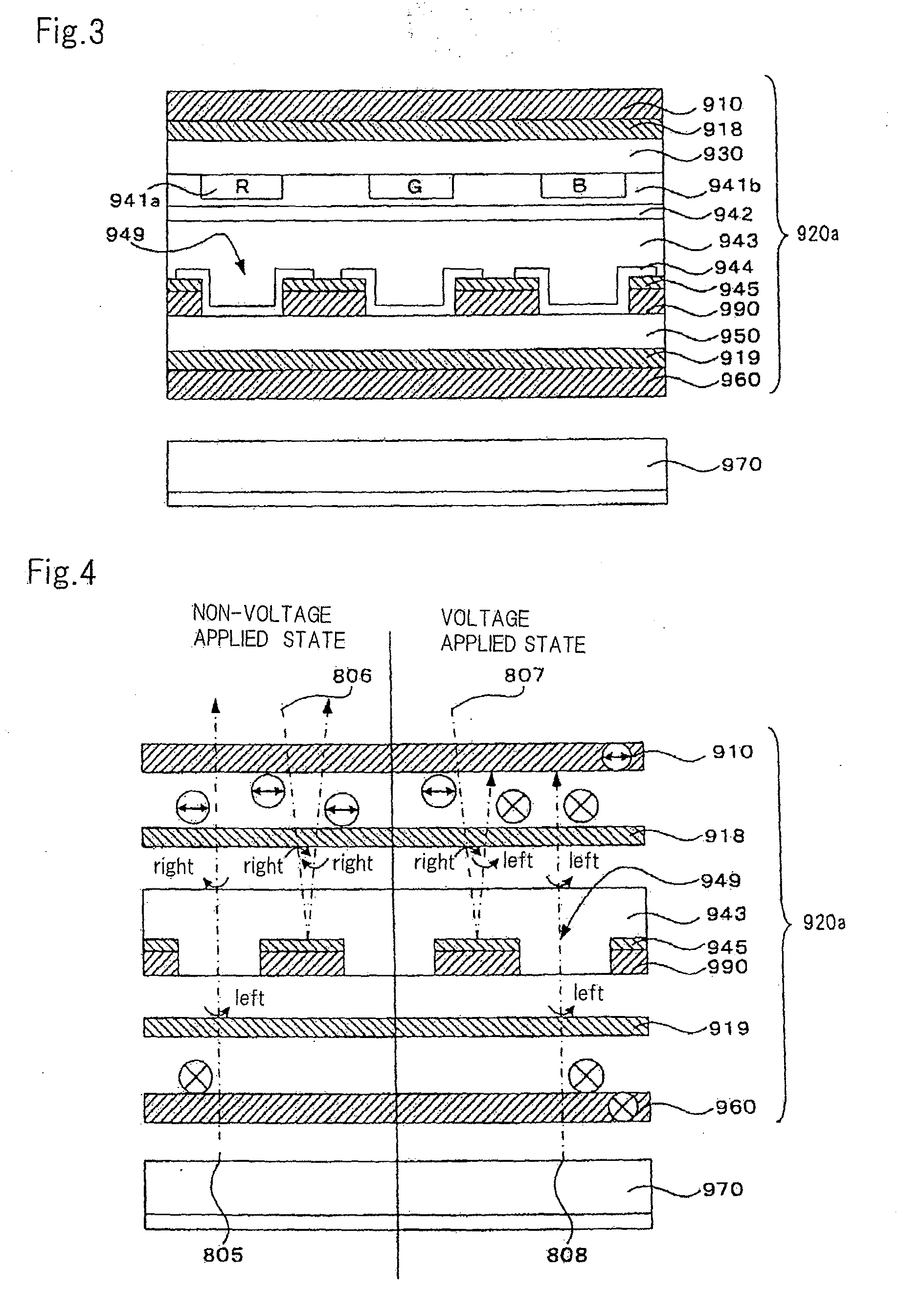
[0164]Referring next to FIGS. 15A and 15B, a description will be given of a liquid crystal display device according to a second embodiment of the present invention. The liquid crystal display device according to this embodiment is configured in a manner similar to the liquid crystal display device according to the first embodiment except for the waveforms of the voltages which are applied for driving the liquid crystal display device. Therefore, the following description will be given with reference to the drawings which were used for describing the configuration of the liquid crystal display device according to the first embodiment.
[0165]Referring first to FIG. 15A, a description will be given of the display mode of this liquid crystal display device. FIG. 15A shows the waveforms of voltages VG, VD, and VCOM which are applied to gate line 253, drain line 252, and common electrode 205, respectively, during G1 duration in the display mode.
[0166]The value of VG is set to VGH only during Gn duration for selecting a sub-pixel connected to each gate line 253 (Gn) and to VGL during the remaining durations. Specifically, the value of VG at G1 is VGH only during G1 duration, and VGL during the remaining durations. The value of VD can be determined within a range of VDL or higher to VDH or lower.
[0167]VCOM presents a common waveform both in the display mode and mirror mode. VCOM takes the values of VCH and VCL which are alternated every two durations, and are also alternated every frame. Specifically, in the frame shown in FIG. 15A, VCOM has the value of VCL in G1 duration and G2 duration and VCH in G3 duration and G4 duration, and in the next frame, VCOM has the value of VCH in G1 duration and G2 duration, and VCL in G3 duration and G4 duration.
[0168]It is assumed in this embodiment that VDH=VCH and VDL=VCL. More specifically, VDH=6V, VDL=1V, VCH=6V, and VCL=1V.
[0169]During G1 duration in the frame shown in FIG. 15A, a voltage having the value of (VD−VCL) is applied between transmission sub-pixel electrode 211 and common electrode 205 of transmission sub-pixel 254 connected to G1. Since the value of VD is equal to or higher than VCL in any transmission sub-pixel 254, a voltage having the value of 0 V or higher should be applied between transmission sub-pixel electrode 211 and common electrode 205.
[0170]Accordingly, transmission sub-pixel 254 connected to G1 at this time is in an image display state, where a positive voltage can be applied between transmission sub-pixel electrode 211 and common electrode 205 by adjusting the value of VD.
[0171]Also, during G3 duration in the frame shown in FIG. 15A, a voltage having the value of (VD−VCH) is applied between transmission sub-pixel electrode 211 and common electrode 205 of transmission sub-pixel 254 connected to G3. Since the value of VD is equal to or lower than VCH in any transmission sub-pixel 254, a voltage having the value of 0 V or lower should be applied between transmission sub-pixel electrode 211 and common electrode 205.
[0172]Accordingly, transmission sub-pixel 254 connected to G1 at this time is in an image display state, where a negative voltage can be applied between transmission sub-pixel electrode 211 and common electrode 205 by adjusting the value of VD.
[0173]Also, during Gn duration in the frame shown in FIG. 15A, the voltage applied between transmission sub-pixel electrode 211 and common electrode 205 of transmission sub-pixel 254 connected to gate line 253 (Gn) alternates between 0 V or higher and 0 V or lower subsequent to G1 and G3 durations as well. Accordingly, any of transmission sub-pixels 254 connected to Gn at this time is in an image display state.
[0174]During G1 duration in the frame next to that shown in FIG. 15A, a voltage having the value of (VD−VCH) is applied between transmission sub-pixel electrode 211 and common electrode 205 of transmission sub-pixel 254 connected to G1. Since the value of VD is equal to or lower than VCH in any of transmission sub-pixels 254, a voltage having the value of 0 V or lower should be applied between transmission sub-pixel electrode 211 and common electrode 205.
[0175]Accordingly, transmission sub-pixel 254 connected to G1 at this time is in an image display state, where a negative voltage can be applied between transmission sub-pixel electrode 211 and common electrode 205 by adjusting the value of VD.
[0176]Also, during G3 duration in the frame next to that shown in FIG. 15A, a voltage having the value of (VD−VCL) is applied between transmission sub-pixel electrode 211 and common electrode 205 of transmission sub-pixel 254 connected to G3. Since the value of VD is equal to or higher than VCL in any transmission sub-pixel 254, a voltage having the value of 0 V or higher should be applied between transmission sub-pixel electrode 211 and common electrode 205.
[0177]Accordingly, transmission sub-pixel 254 connected to G1 at this time is in an image display state, where a positive voltage can be applied between transmission sub-pixel electrode 211 and common electrode 205 by adjusting the value of VD.
[0178]Also, during Gn duration in the frame next to that shown in FIG. 15A, the voltage applied between transmission sub-pixel electrode 211 and common electrode 205 of transmission sub-pixel 254 connected to gate line 253 (Gn) alternates between 0 V or lower and 0 V or higher subsequent to G1 and G3 durations as well. Accordingly, any of transmission sub-pixels 254 connected to Gn at this time is in an image display state.
[0179]As described above, this liquid crystal display device employs the gate line inversion driving method, like the liquid crystal display device according to the first embodiment, but differs from the liquid crystal display device according to the first embodiment by simply focusing attention only on transmission sub-pixel 254 in the display mode, in that the polarity of the voltage applied between transmission sub-pixel electrode 211 and common electrode 205 is inverted for every gate line 253, and is also inverted every frame. Since the polarity of the voltage applied between transmission sub-pixel electrode 211 and common electrode 205 is inverted for every gate line 253 in the display mode, flickers are less prominent even when the frame period is short.
[0180]During Gn duration in the display mode of this liquid crystal display device, the value of VD is made equal to the value of VCOM in any of mirror sub-pixels 255 connected to Gn. In this way, a voltage having the value of 0 V is applied between mirror sub-pixel electrode 212 and common electrode 205 in any of mirror sub-pixels 255, so that mirror sub-pixel 255 is placed into a non-voltage applied state and therefore a non-mirror state.
[0181]This liquid crystal display device can place transmission sub-pixels 254 into an image display state and mirror sub-pixels 255 into a non-mirror state by driving sub-pixels 254, 255 in the foregoing manner. In this way, this liquid crystal display device can realize the display mode.
[0182]Referring next to FIG. 15B, a description will be given of the mirror mode of this liquid crystal display device. FIG. 15B shows the waveforms of voltages VG, VD, and VCOM applied to gate line 253, drain line 252, and common electrode 205, respectively, during G1 duration in the mirror mode.
[0183]The value of VG is set to VGH only during Gn duration for selecting a sub-pixel connected to each gate line 253 (Gn) and to VGL during the remaining durations. Specifically, the value of VG at G1 is VGH only during G1 duration, and VGL during the remaining durations.
[0184]VD takes the values of VDH and VDL which are alternated every two durations and also are alternated every frame. Further, VD presents a waveform which is shifted by one duration from the waveform of VCOM. Specifically, the value of VD is VDL during G1 duration, and VDH during G2 duration and G3 duration in the frame shown in FIG. 15B, and the value of VD is VCH during G1 duration, and VCL during G2 duration and G3 duration in the next frame.
[0185]Notably, in this embodiment, since a phase difference of λ/4 must be given to light which is transmitted liquid crystal layer 206 in mirror sub-pixel 255 in a voltage applied state, the value of VD is set to VD1 lower than VDH or to VD2 higher than VDL during a period (G2 duration, G4 duration, . . . ) for selecting gate electrode 253 connected to mirror sub-pixel 255. In this embodiment, VD1=4V, and VD2=3V.
[0186]During G1 duration in the frame shown in FIG. 15B, a voltage having the value of (VD−VCL) is applied between transmission sub-pixel electrode 211 and common electrode 205 of transmission sub-pixel 254 connected to G1. Since the value of VD is VDL in any transmission sub-pixel 254, a voltage having the value of 0 V is applied between transmission sub-pixel electrode 211 and common electrode 205. Accordingly, since any one of transmission sub-pixels 254 connected to G1 at this time is placed into a non-voltage applied state, this one sub-pixel presents a black display state.
[0187]Also, during G3 duration in the frame shown in FIG. 15B, a voltage having the value of (VD−VCH) is applied between transmission sub-pixel electrode 211 and common electrode 205 of transmission sub-pixel 254 connected to G3. Since the value of VD is equal to VDH in any transmission sub-pixel 254, a voltage having the value of 0 V should be applied between transmission sub-pixel electrode 211 and common electrode 205. Accordingly, transmission sub-pixel 254 connected to G3 at this time presents a black display state because any of transmission sub-pixels 254 connected to G3 at this time is placed into a non-voltage applied state.
[0188]Also, during Gn duration in the frame shown in FIG. 15B, since the value of VD is also equal to the value of VCOM during Gn duration in transmission sub-pixels 254 connected to gate lines 253 (Gn) except for G1 and G3, a voltage having the value of 0 V should be applied between transmission sub-pixel electrode 211 and common electrode 205. Accordingly, since any one of transmission sub-pixels 254 connected to Gn at this time is placed into a non-voltage applied state, this one sub-pixel presents a black display state.
[0189]During G1 duration in the frame next to that shown in FIG. 15B, a voltage having the value of (VD−VCH) is applied between transmission sub-pixel electrode 211 and common electrode 205 of transmission sub-pixel 254 connected to G1. Since the value of VD is equal to VDH in any of transmission sub-pixels 254, a voltage having the value of 0 V should be applied between transmission sub-pixel electrode 211 and common electrode 205. Accordingly, since any one of transmission sub-pixels 254 connected to G1 at this time is placed into a non-voltage applied state, this one sub-pixel presents a black display state.
[0190]Also, during G3 duration in the frame next to that shown in FIG. 15B, a voltage having the value of (VD−VCL) is applied between transmission sub-pixel electrode 211 and common electrode 205 of transmission sub-pixel 254 connected to G3. Since the value of VD is equal to VDL in any transmission sub-pixel 254, a voltage having the value of 0 V should be applied between transmission sub-pixel electrode 211 and common electrode 205. Accordingly, since any of transmission sub-pixels 254 connected to G3 at this time is placed into a non-voltage applied state, it presents a black display state.
[0191]Also, during Gn duration in the frame next to that shown in FIG. 15B, since the value of VD at Gn is also equal to the value of VCOM in transmission sub-pixels 254 connected to gate lines 253 (Gn) other than G1 and G3, a voltage having the value of 0 V should be applied between transmission sub-pixel electrode 211 and common electrode 205. Accordingly, since any one of transmission sub-pixels 254 connected to Gn at this time is placed into a non-voltage applied state, this one sub-pixel presents a black display state.
[0192]During G2 duration in the frame shown in FIG. 15B, a voltage having the value of (VD−VCL) is applied between mirror sub-pixel electrode 212 and common electrode 205 of mirror sub-pixel 255 connected to G2. Since the value of VD is equal to VD1 in any of mirror sub-pixels 255, a voltage having the value of (VD1−VCL) is applied between mirror sub-pixel electrode 212 and common electrode 205. In this event, since any one of mirror sub-pixels 255 is placed into a voltage applied state, this one sub-pixel presents a mirror state.
[0193]Also, during G4 duration in the frame shown in FIG. 15B, a voltage having the value of (VD−VCH) is applied between mirror sub-pixel electrode 212 and common electrode 205 of mirror sub-pixel 255 connected to G4. Since the value of VD is equal to VD2 in any of mirror sub-pixels 255, a voltage having the value of (VD2−VCH) is applied between mirror sub-pixel electrode 212 and common electrode 205. In this event, since any one of mirror sub-pixels 255 is placed into a voltage applied state, this one sub-pixel presents a mirror state.
[0194]Also, during Gn duration in the frame shown in FIG. 15B, the voltage applied between transmission sub-pixel electrode 211 and common electrode 205 of transmission sub-pixel 254 connected to gate line 253 (Gn) alternates between 0 V or higher and 0 V or lower subsequent to G1 and G3 durations as well. Accordingly, any one of transmission sub-pixels 254 connected to Gn at this time is in an image display state.
[0195]During G2 duration in the frame next to that shown in FIG. 15B, a voltage having the value of (VD−VCH) is applied between mirror sub-pixel electrode 212 and common electrode 205 of mirror sub-pixel 255 connected to G2. Since the value of VD is equal to VD2 in any of mirror sub-pixels 255, a voltage having the value of (VD2−VCH) is applied between mirror sub-pixel electrode 212 and common electrode 205. In this event, since any one of mirror sub-pixels 255 is placed into a voltage applied state, this one sub-pixel presents a mirror state.
[0196]Also, during G4 duration in the frame next to that shown in FIG. 15B, a voltage having the value of (VD−VCL) is applied between mirror sub-pixel electrode 212 and common electrode 205 of mirror sub-pixel 255 connected to G4. Since the value of VD is equal to VD1 in any of mirror sub-pixels 255, a voltage having the value of (VD1−VCL) is applied between mirror sub-pixel electrode 212 and common electrode 205. In this event, since any one of mirror sub-pixels 255 is placed into a voltage applied state, this one sub-pixel presents a mirror state.
[0197]Also, during Gn duration in the frame next to that shown in FIG. 15B, a negative voltage and a positive voltage are alternately applied between transmission sub-pixel electrode 211 and common electrode 205 of transmission sub-pixel 254 connected to gate line 253 (Gn) subsequent to G2 and G4 durations as well. Accordingly, any one of mirror sub-pixels 255 connected to Gn at this time is in a mirror state.
[0198]As described above, this liquid crystal display device employs the gate line inversion driving method, like the liquid crystal display device according to the first embodiment, but differs from the liquid crystal display device according to the first embodiment in that the polarity of the voltage applied between mirror sub-pixel electrode 212 and common electrode 205 is inverted every gate line 253, and is also inverted every frame, as can be recognized by simply focusing attention only on mirror sub-pixel 255 in the mirror mode.
[0199]This liquid crystal display device can place transmission sub-pixels 254 into a black display state as well as place mirror sub-pixels 255 into a mirror state by driving sub-pixels 254, 255 in the foregoing manner. In this way, this liquid crystal display device can realize the mirror mode.
Example
Third Embodiment
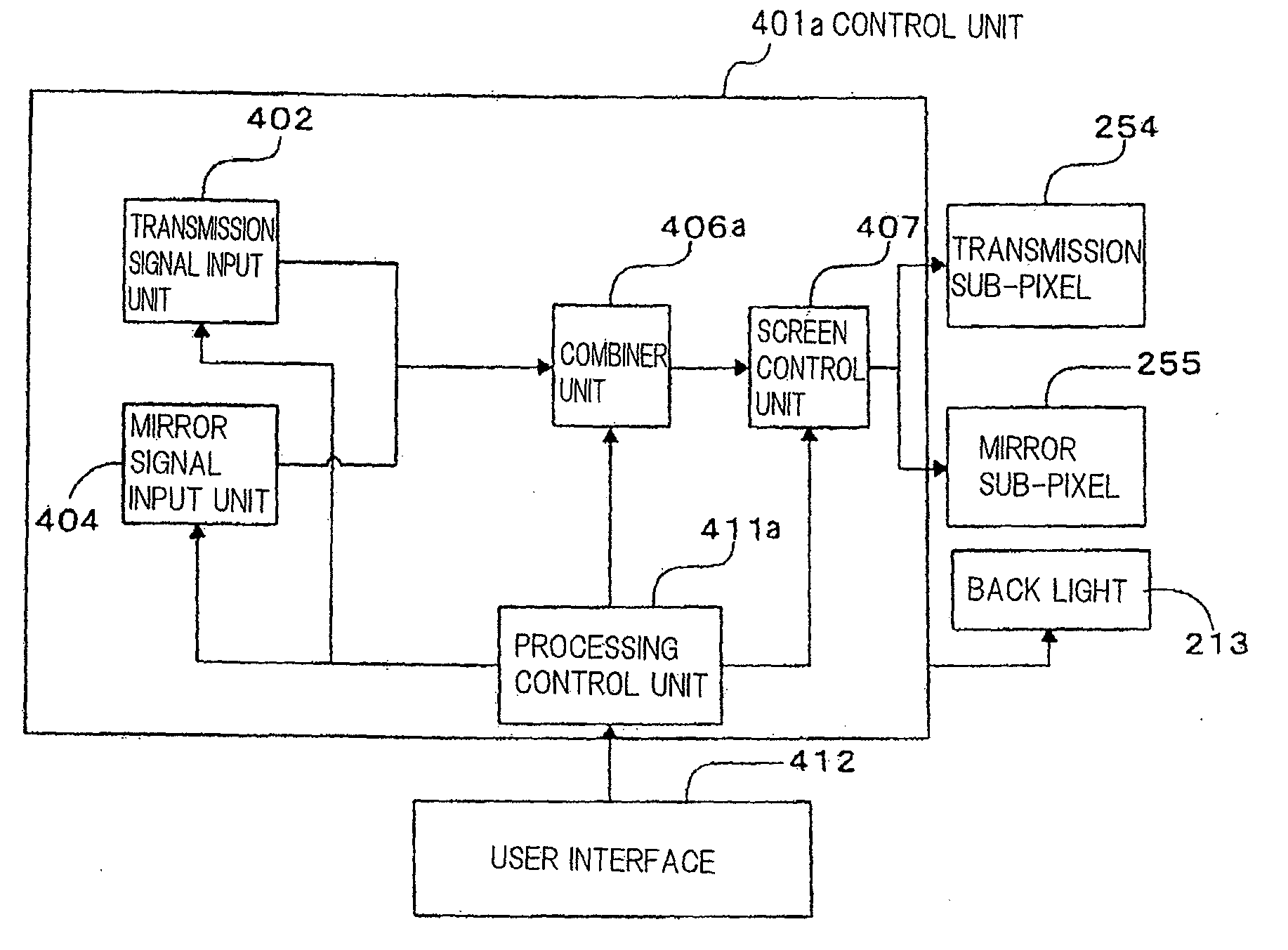
[0200]Referring next to FIGS. 16 and 17, a description will be given of a liquid crystal display device according to a third embodiment of the present invention. The liquid crystal display device according to this embodiment is constructed in a manner similar to the liquid crystal display device according to the first embodiment except for the control unit. FIGS. 16 and 17 correspond to FIGS. 9 and 10 in the first embodiment, where the same components are designated by the same reference numerals.
[0201]FIG. 16 is a block diagram showing a screen control function of the liquid crystal display device, and FIG. 17 is a diagram showing an example of screen control process in accordance with the screen control function. FIG. 17 shows a screen control process in the screen mode shown in FIG. 8A as an example of the screen control.
[0202]This liquid crystal display device does not comprise combiner units 403, 405 shown in FIG. 9.
[0203]Specifically, combiner unit 406a combines image display information 301 and black display information 304 applied thereto from display signal input unit 402 and non-mirror information 302 and mirror information 305 applied thereto from mirror signal input unit 404 into screen control information 316a based on a transmission position signal and a mirror position signal applied thereto from processing control unit 411a.
[0204]Then, combiner unit 406a sends screen control information 316a to screen control unit 407, such that screen control unit 407 drives transmission sub-pixels 254 and mirror sub-pixel 255 in accordance with screen control information 316a.
[0205]In this embodiment, for example, transmission sub-pixel information 313 (see FIG. 10) which represents a mixture of an image display state and a black display state cannot be created from image display information 301 and black display information 304. However, a screen mode for mixing the display mode with the mirror mode can also be implemented in this embodiment by applying transmission signal input unit 402 with previously combined transmission sub-pixel information 313 from processing control unit 411, and recording previously combined transmission sub-pixel information 314 in a memory of mirror signal input unit 404. Consequently, control unit 401a can conduct the image control in the other screen modes as shown, for example, in FIGS. 8B-8E in a similar manner.
Login to view more PUM


Description & Claims & Application Information
We can also present the details of the Description, Claims and Application information to help users get a comprehensive understanding of the technical details of the patent, such as background art, summary of invention, brief description of drawings, description of embodiments, and other original content. On the other hand, users can also determine the specific scope of protection of the technology through the list of claims; as well as understand the changes in the life cycle of the technology with the presentation of the patent timeline. Login to view more.
Login to view more Similar technology patents
Image encoding apparatus and method, computer program, and computer-readable storage medium
InactiveUS20060050974A1High image qualityCharacter and pattern recognitionDigital video signal modificationNonlinear boundaryJPEG
Owner:CANON KK
Camera shooting lens
Owner:ZHEJIANG SUNNY OPTICAL CO LTD
Optical imaging lens
Owner:ZHEJIANG SUNNY OPTICAL CO LTD
Imaging method and image forming apparatus
ActiveUS20080068412A1High image qualityMechanical cleaningPressure cleaningRecording headEngineering
Owner:RICOH KK
Classification and recommendation of technical efficacy words
- High image quality
Device for expanding an exit pupil in two dimensions
ActiveUS20100321781A1High image qualityEfficient couplingDiffraction gratingsCoupling light guidesPhysicsExit pupil
Owner:MAGIC LEAP
Portable DVD player
InactiveUS20050053365A1Easy to use and transportHigh image qualityCarrier indicating/warning arrangementsTelevision system detailsDVD playerEngineering
Owner:DVDO
Camera module
ActiveUS20070183773A1High image qualityTelevision system detailsColor television detailsSolid-stateEngineering
Owner:MAXELL HLDG LTD
Solid-state image pickup device and camera
ActiveUS20050259167A1High image qualitySuppress increase of chip areaTelevision system detailsTelevision system scanning detailsSolid-stateAudio power amplifier
Owner:CANON KK
Coverage adaptive multisampling
ActiveUS8044956B1High performanceHigh image qualityDetails involving antialiasingCathode-ray tube indicatorsGeometric primitiveImaging quality
Owner:NVIDIA CORP