Method of manufacturing led lamp

a manufacturing method and led lamp technology, applied in semiconductor/solid-state device manufacturing, electrical equipment, semiconductor devices, etc., can solve the problems of reduced light availability of led chips, uneven surface, and insufficient softening of sealing glass, so as to improve the surface accuracy of forming dies, prevent breakage or misalignment of led elements, and smooth sealing members.

Active Publication Date: 2010-09-30
TOYODA GOSEI CO LTD
View PDF37 Cites 53 Cited by
  • Summary
  • Abstract
  • Description
  • Claims
  • Application Information

AI Technical Summary

Benefits of technology

[0013]According to the method of manufacturing a LED lamp of the invention, since a sealing member is bonded to a substrate by thermal compression in a sealing process so that a LED element is located in a concave portion of the sealing member, the LED element is prevented from being directly pressed when the sealing member is pressed against the substrate. As a result, breakage or misalignment of the LED element is prevented. In addition, since the concave portion is formed on the sealing member prior to the sealing process, it is not necessary to move a forming material of the sealing material equivalent to volume of the LED element in the sealing process, which would be necessary in case of deformation, etc., thus, it is possible to bond by thermal compression at a temperature lower than the conventional art. As described above, since the sealing member is not excessively softened by the thermal compression bonding at a low temperature, the sealing member is prevented from adhering to a forming die which presses the sealing member against the substrate. As a result, it is possible to smooth the surface of the sealing member by increasing the surface accuracy of the forming die and to form a further precise lens shape.

Problems solved by technology

However, roughening the surface as described above is not preferable since surface accuracy of the LED lamp is reduced and light availability of the LED chip decreases.
When the sealing glass is heated at a temperature lower than the softening temperature in order to avoid the above problem, the sealing glass is not sufficiently softened and an excessive force is then applied to the LED chip when the sealing glass is pressed against the substrate.
This caused breakage or misalignment of the LED chip.

Method used


Image

  • Method of manufacturing led lamp
  • Method of manufacturing led lamp
  • Method of manufacturing led lamp

Examples


first embodiment

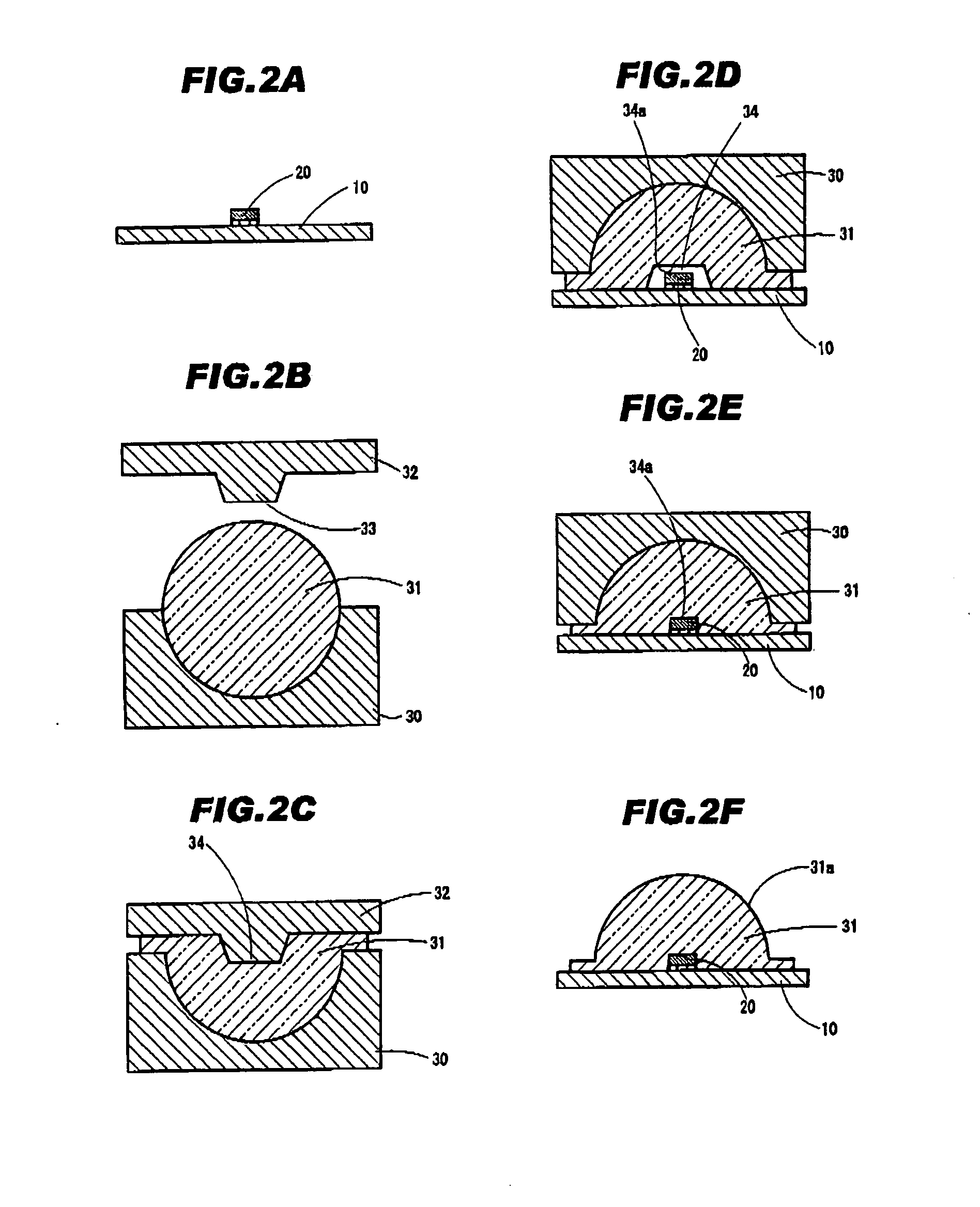
[0098]FIG. 1 is a flow diagram of a first embodiment. FIG. 2 is a schematic vertical cross sectional view for illustrating manufacturing processes in the first embodiment.

[0099]As shown in FIG. 1, a mounting process for flip-chip-mounting a LED element on a substrate (S1), a sealing member preparation process for preparing a sealing member provided with a concave portion capable of housing the LED element (S2), and a sealing process in which the sealing member is arranged so that a forming surface of the concave portion of the sealing member faces the LED element, the sealing member is bonded to the substrate by thermally compressing on the substrate side and the forming surface of the concave portion is made along the LED element (S3) are included.

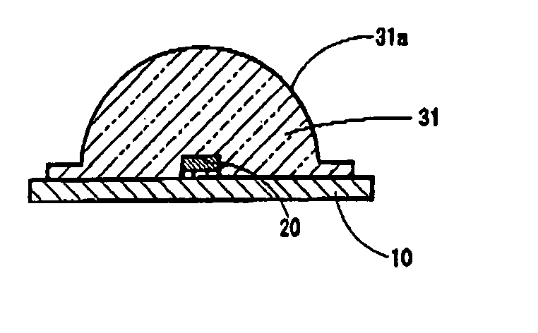
[0100]As shown in FIG. 2(A), a LED element 20 is flip-chip-mounted on a substrate 10 in the mounting process (S1). The substrate 10 is a ceramic substrate. The LED element 20 is a flip-chip type LED element and generates white light. The ...

second embodiment

[0132]FIG. 6 is a schematic vertical cross sectional view for illustrating manufacturing processes in a second embodiment of the invention.

[0133]Firstly, as shown in FIG. 6(A), multiple LED elements 20 (sixteen in this example) are mounted on the substrate 11 by vertically and horizontally arranging in a square pattern at equal intervals. Next, a sealing member 311 is prepared. As shown in FIG. 6(B) which is a cross section taken on line A-A of FIG. 6(A), the sealing member 311 includes plural concave portions 341 having a trapezoidal vertical cross sectional shape at positions facing each of the LED elements 20.

[0134]The sealing member 311 is formed of the same material as the sealing member 31 and the concave portion 341 is formed in the same manner as the concave portion 34 of the sealing member 31.

[0135]Then, as shown in FIG. 6(C), the sealing member 311 is arranged on the substrate 11 so that the concave portion 341a of each concave portion 341 encloses the corresponding LED el...

third embodiment

[0139]FIG. 7 is a schematic vertical cross sectional view for illustrating manufacturing processes in a third embodiment.

[0140]The third embodiment is different from the second embodiment (see FIG. 6) in that, as shown in FIG. 7(A), (a) a sealing member 312 provided with a lens forming portion (main body) 312a having a concave portion 341 and a basal portion 312b connecting the adjacent lens forming portions (main bodies) 312a and bonded to the substrate 10 by pressure is used instead of the sealing member 311 and (b) an upper die (sealing member forming die) 301 provided with concave portions 301a along the lens forming portions (main bodies) 312a of the sealing member 312 is used instead of the upper die 300.

[0141]The sealing member 312 is formed of the same material as the sealing member 311.

[0142]Then, as shown in FIG. 7(B), the basal portion 312b of the a sealing member 321 is bonded to the substrate 11 by thermal compression by pressing down the upper die 301. After that, indi...


PUM

PropertyMeasurementUnit
temperatureaaaaaaaaaa
Tgaaaaaaaaaa
Tgaaaaaaaaaa

Abstract

A method of manufacturing a LED lamp that is formed by sealing a LED element mounted on a substrate with glass, includes a mounting process for mounting the LED element on the substrate, a sealing member preparation process for preparing a glass sealing member that includes a concave portion being capable of housing the LED element, and a sealing process wherein the sealing member is arranged so that a forming surface of the concave portion faces the LED element, the sealing member is bonded to the substrate by thermal compression bonding, and the forming surface of the concave portion is made along the LED element.

Description

[0001]The present application is based on Japanese Patent Application Nos. 2009-076907, 2009-204043 and 2009-298785 filed on Mar. 26, 2009, Sep. 3, 2009 and Dec. 28, 2009, respectively, the entire contents of which are incorporated herein by reference.BACKGROUND OF THE INVENTION[0002]1. Field of the Invention[0003]The invention relates to a method of manufacturing a LED lamp.[0004]2. Description of the Related Art[0005]Conventionally, a method, in which a LED chip is sealed by pressing a plate glass softened by heat against a substrate having the LED chip thereon using a forming die, is broadly used as a method of sealing a LED chip with glass. A LED lamp sealed with glass by such a method is disclosed in WO 2004 / 082036 and JP 2008-124153. In addition, JP 2008-49841 discloses a method in which a concave portion for covering a LED chip is provided in a sealing glass in order to prevent the sealing glass from contacting with the LED chip, the LED chip is then covered by the sealing gl...

Claims


Application Information

Patent Timeline
Patent Type & Authority Applications(United States)
IPC IPC(8): H01L33/52H01L33/48
CPCB29C43/021B29C43/18B29K2709/08H01L33/54H01L33/56H01L2933/005H01L2224/48091H01L2924/12041H01L24/97H01L2224/49107H01L2924/00014H01L2924/00H01L2924/15787
Inventor WADA, SATOSHIMORIYAMA, MIKI
Owner TOYODA GOSEI CO LTD
Why Eureka
Try Eureka