
Method of maintaining the state of semiconductor memory having electrically floating body transistor

a technology of floating body transistor and semiconductor memory, which is applied in the field of maintaining the state of semiconductor memory device/array of devices having an electrically floating body transistor, can solve the problems of dram memory cell still needing refresh operation, interrupting access to memory cells being refreshed, and difficult to solv

Active Publication Date: 2010-09-30
ZENO SEMICON
View PDF80 Cites 244 Cited by
  • Summary
  • Abstract
  • Description
  • Claims
  • Application Information

AI Technical Summary

Benefits of technology

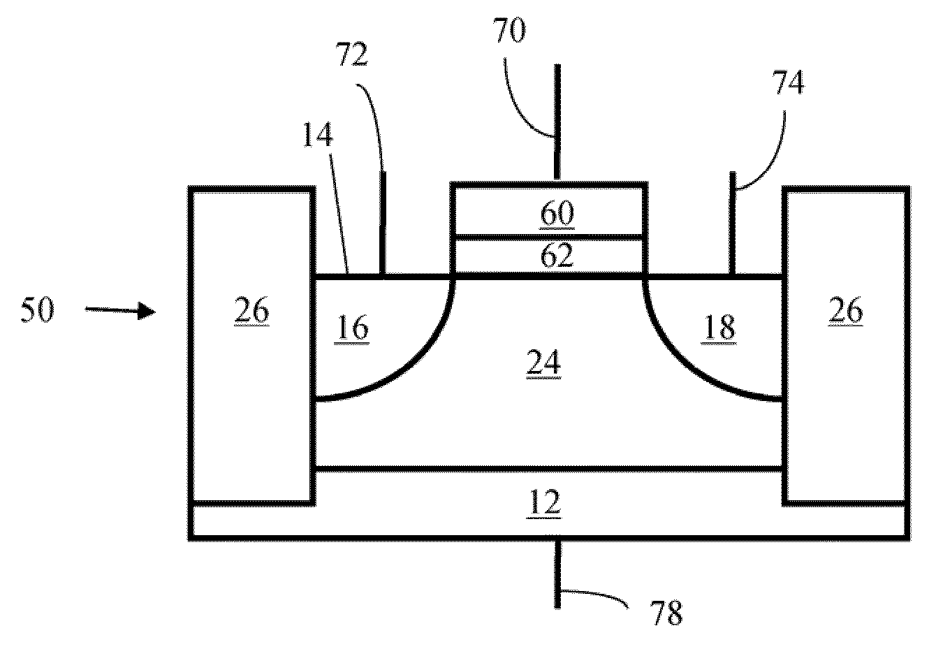
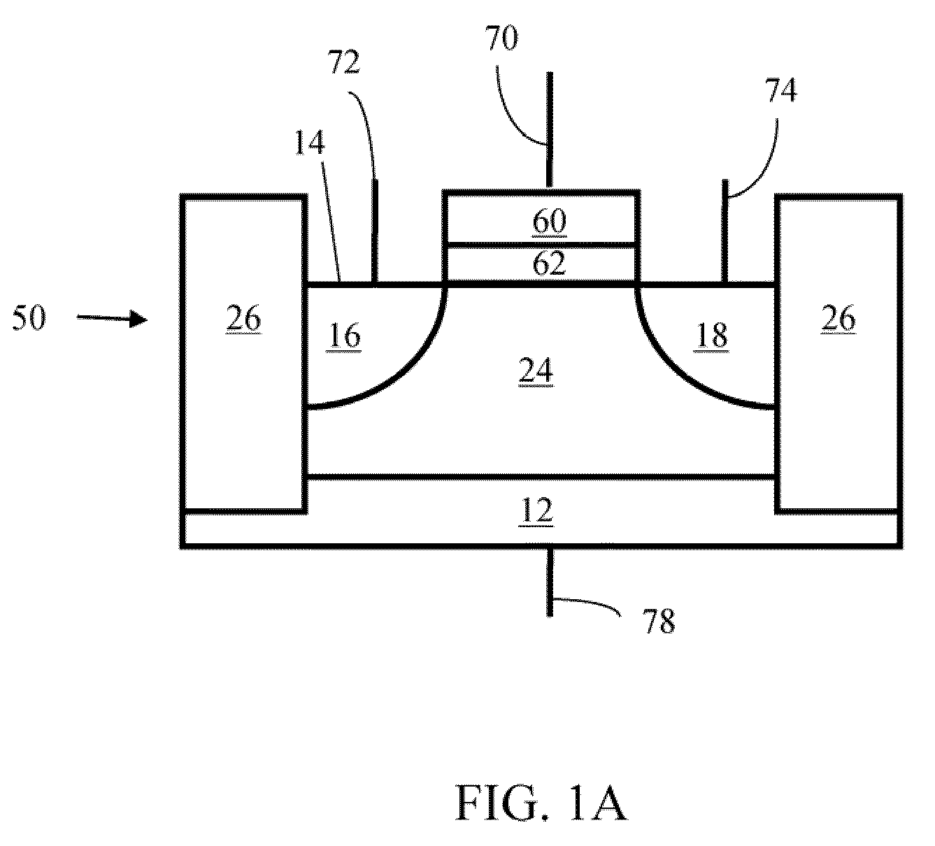
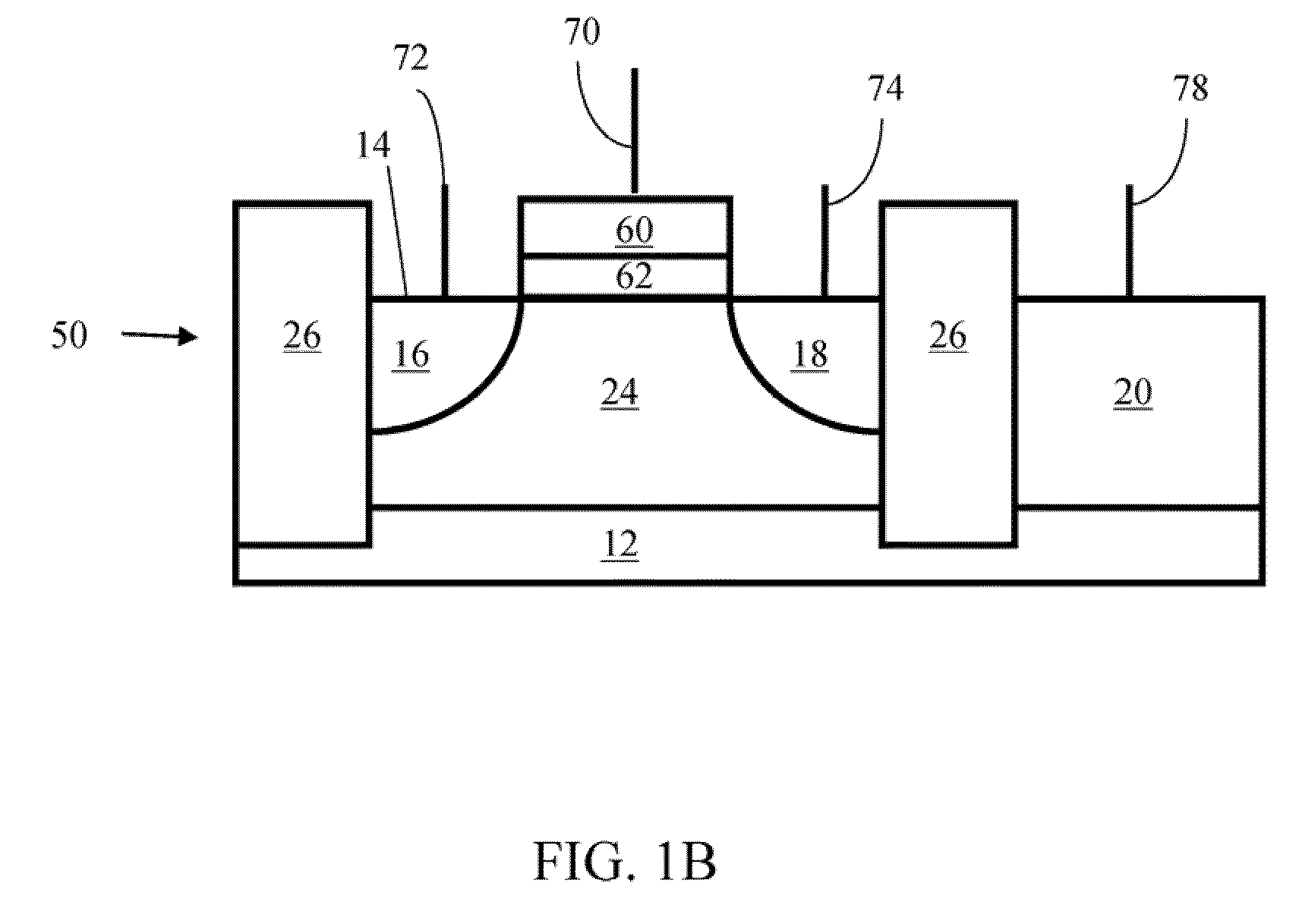
The present invention provides a method for maintaining the state of a memory cell without interrupting access to the cell. The method includes applying a back bias to the cell to offset charge leakage out of the floating body region of the cell. The back bias can be applied as a constant positive voltage or as a periodic pulse of voltage. The method also includes performing a holding operation on all or a portion of the cells in the array, while simultaneously accessing another cell. The holding operation can be performed using the back bias applied to a terminal not used for memory address selection. The method can be used in multi-level cell arrays to selectively store data in a specific cell. The refreshing of a state of a memory cell can be performed without alternating read and write operations. Overall, the method provides a way to maintain the state of a memory cell without interrupting access to it, which can improve the memory's performance and reliability.

Problems solved by technology

As the 1T / 1C memory cell feature is being scaled, difficulties arise due to the necessity of maintaining the capacitance value.
However, unlike SRAM, such DRAM memory cell still requires refresh operation, since the stored charge leaks over time.
However, such operation still interrupts access to the memory cells being refreshed.

Method used


Image

  • Method of maintaining the state of semiconductor memory having electrically floating body transistor
  • Method of maintaining the state of semiconductor memory having electrically floating body transistor
  • Method of maintaining the state of semiconductor memory having electrically floating body transistor

Examples


Embodiment Construction

[0111]Before the present systems, devices and methods are described, it is to be understood that this invention is not limited to particular embodiments described, as such may, of course, vary. It is also to be understood that the terminology used herein is for the purpose of describing particular embodiments only, and is not intended to be limiting, since the scope of the present invention will be limited only by the appended claims.

[0112]Where a range of values is provided, it is understood that each intervening value, to the tenth of the unit of the lower limit unless the context clearly dictates otherwise, between the upper and lower limits of that range is also specifically disclosed. Each smaller range between any stated value or intervening value in a stated range and any other stated or intervening value in that stated range is encompassed within the invention. The upper and lower limits of these smaller ranges may independently be included or excluded in the range, and each...


PUM


Abstract

Methods of maintaining a state of a memory cell without interrupting access to the memory cell are provided, including applying a back bias to the cell to offset charge leakage out of a floating body of the cell, wherein a charge level of the floating body indicates a state of the memory cell; and accessing the cell.

Description

CROSS-REFERENCE[0001]This application is a continuation-in-part application of co-pending application Ser. No. 12 / 552,903, filed Sep. 2, 2009, which is a continuation-in-part application of application Ser. No. 11 / 998,311, filed Nov. 29, 2007, and a continuation-in-part application of application Ser. No. 12 / 533,661, filed Jul. 31, 2009, and a continuation-in-part application of application Ser. No. 12 / 545,623, filed Aug. 21, 2009, and which claims the benefit of U.S. Provisional Application No. 61 / 093,726, filed Sep. 3, 2008, and U.S. Provisional Application No. 61 / 094,540, filed Sep. 5, 2008. We hereby incorporate all of the aforementioned application herein, in their entireties, by reference thereto, and we claim priority to application Ser. Nos. 12 / 552,903; 11 / 998,311; 12 / 533,661 and 12 / 545,623, under 35 USC §120.[0002]This application claims the benefit of U.S. Provisional Application. No. 61 / 309,589, filed Mar. 2, 2010, which application is hereby incorporated herein, in its e...

Claims


Application Information

Patent Timeline
Patent Type & Authority Applications(United States)
IPC IPC(8): G11C7/10G11C7/00H10B12/00
CPCG11C11/404G11C11/565G11C14/0018G11C16/0416G11C2211/4016H01L27/108G11C11/4094H01L29/66825H01L29/66833H01L29/7841H01L29/7881G11C7/00H01L27/10802G11C11/4074G11C11/4096G11C11/4099H10B12/20H10B12/00H10B12/10G11C11/4067G11C11/409H01L29/0821H01L29/1004H01L29/7395H01L29/7455
Inventor WIDJAJA, YUNIARTOOR-BACH, ZVI
Owner ZENO SEMICON
Learn More