Semiconductor memory device having electrically floating body transistor, semiconductor memory device having both volatile and non-volatile functionality and method or operating
What is AI technical title?
AI technical title is built by Patsnap AI team. It summarizes the technical point description of the patent document.
a semiconductor memory and transistor technology, applied in the field of semiconductor memory devices, can solve the problems of interrupting the access to the memory cells being refreshed, dram memory cells still need refresh operation, and difficulties arise due to the operation of dram memory cells
Active Publication Date: 2015-10-06
ZENO SEMICON
View PDF122 Cites 111 Cited by
Summary
Abstract
Description
Claims
Application Information
AI Technical Summary
This helps you quickly interpret patents by identifying the three key elements:
Problems solved by technology
Method used
Benefits of technology
Benefits of technology
The patent describes a method for maintaining a memory cell without interrupting access to it. This is done by applying a back bias to the cell to prevent charge leakage from the floating body of the cell. The charge level of the floating body indicates the state of the memory cell. This method increases the maximum potential that can be stored in the floating body, resulting in a larger memory window. An integrated circuit that includes several such memory cells connected either in series or in parallel is also provided, which offers a compact memory array.
Problems solved by technology
As the 1T / 1C memory cell feature is being scaled, difficulties arise due to the necessity of maintaining the capacitance value.
However, unlike SRAM, such DRAM memory cell still requires refresh operation, since the stored charge leaks over time.
However, such operation still interrupts access to the memory cells being refreshed.
In addition, non-volatile memory devices can only perform limited number of cycles, often referred to as endurance cycle limitation.
Method used
Image
Click on the blue label to locate the original text in one second.
Reading with bidirectional positioning of images and text.
Examples
Embodiment Construction
[0423]Before the present systems, devices and methods are described, it is to be understood that this invention is not limited to particular embodiments described, as such may, of course, vary. It is also to be understood that the terminology used herein is for the purpose of describing particular embodiments only, and is not intended to be limiting, since the scope of the present invention will be limited only by the appended claims.
[0424]Where a range of values is provided, it is understood that each intervening value, to the tenth of the unit of the lower limit unless the context clearly dictates otherwise, between the upper and lower limits of that range is also specifically disclosed. Each smaller range between any stated value or intervening value in a stated range and any other stated or intervening value in that stated range is encompassed within the invention. The upper and lower limits of these smaller ranges may independently be included or excluded in the range, and each...
PUM
Abstract
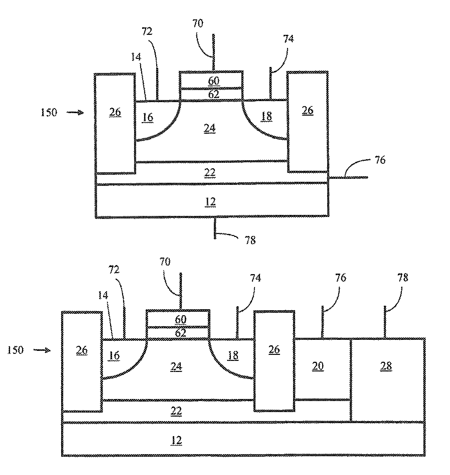
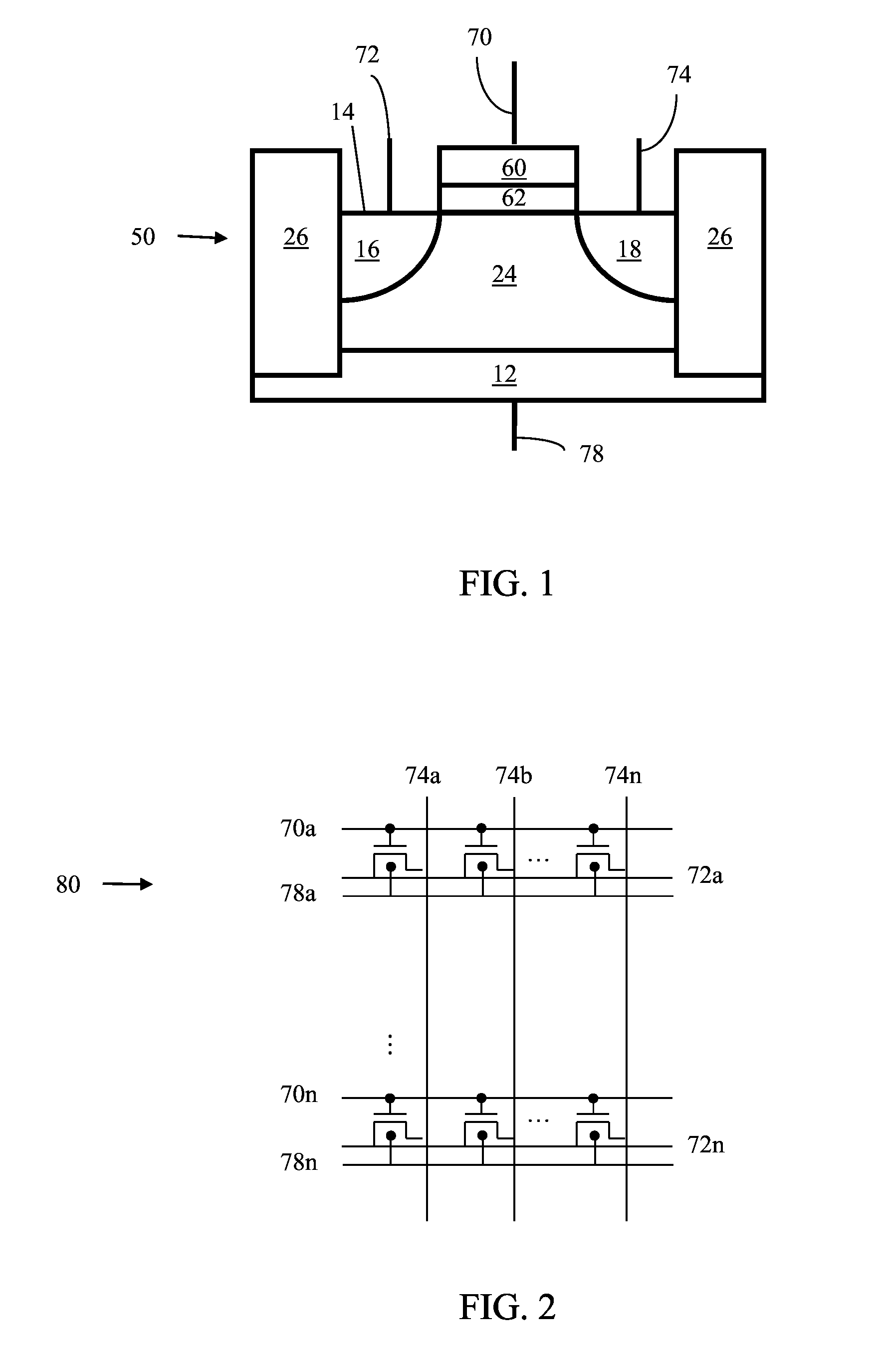
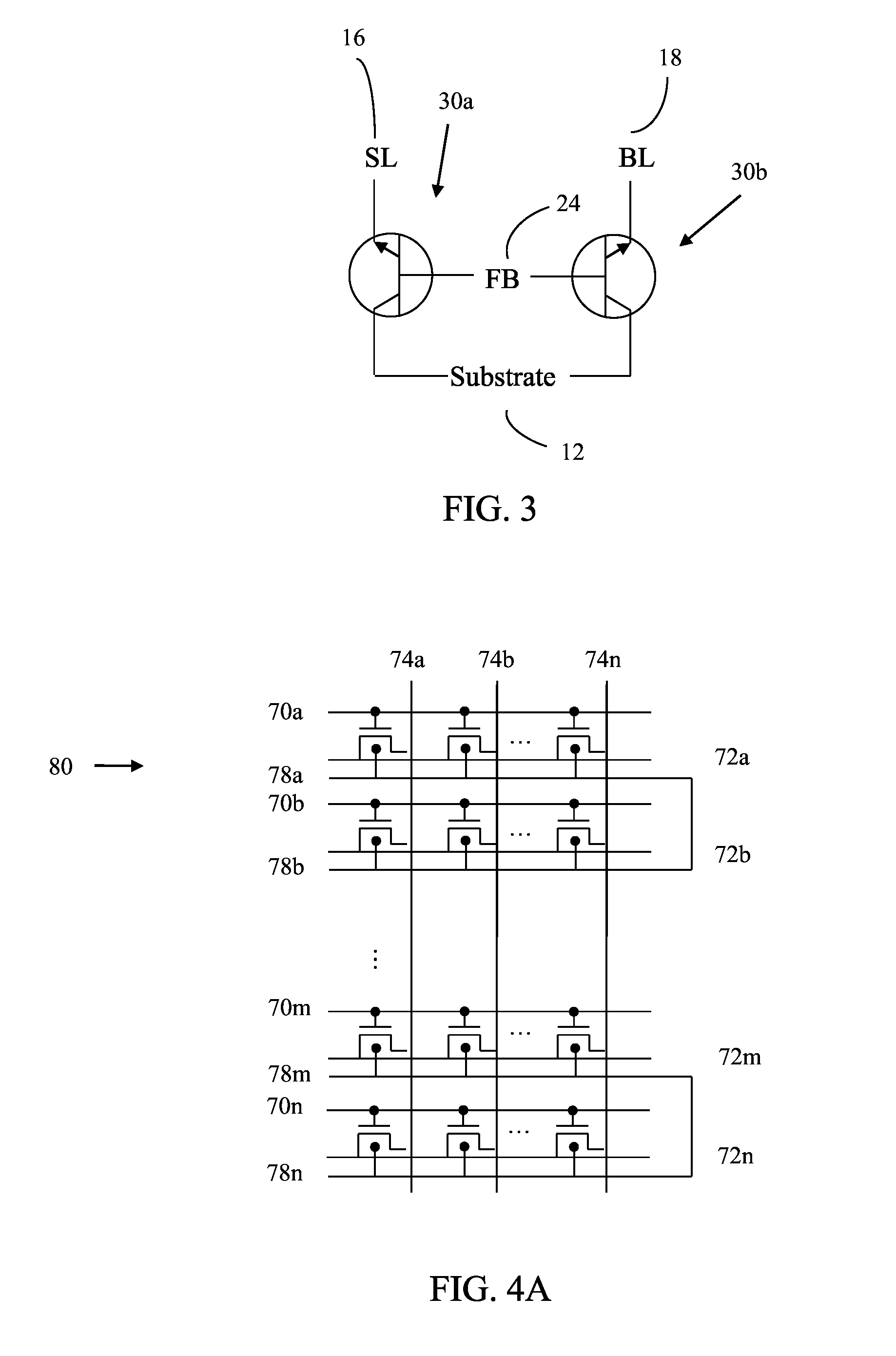
A semiconductormemory cell includes a floating body region configured to be charged to a level indicative of a state of the memory cell; a first region in electrical contact with said floating body region; a second region in electrical contact with said floating body region and spaced apart from said first region; and a gate positioned between said first and second regions. The cell may be a multi-level cell. Arrays of memory cells are disclosed for making a memory device. Methods of operating memory cells are also provided.
Description
CROSS-REFERENCE[0001]This application is a 371 filing and claims the benefit under 35 USC 371(c) of PCT Application No. PCT / US2011 / 023947, filed Feb. 7, 2011 which claims the benefit of U.S. Provisional Application No. 61 / 302,129, filed Feb. 7, 2010, and U.S. Provisional Application No. 61 / 425,820, filed Dec. 22, 2010, and which PCT Application is an international filing of application Ser. No. 12 / 897,528, filed Oct. 4, 2010, now U.S. Pat. No. 8,514,622 issued on Aug. 20, 2013; Ser. No. 12 / 797,320 filed Jun. 9, 2012, now U.S. Pat. No. 8,130,548 issued on Mar. 6, 2012; Ser. No. 12 / 797,334, filed Jun. 9, 2010, now U.S. Pat. No. 8,130,547, issued on Mar. 6, 2012; Ser. No. 12 / 897,516, filed Oct. 4, 2010, now U.S. Pat. No. 8,547,756, issued on Oct. 1, 2013 and Ser. No. 12 / 897,538, filed Oct. 4, 2012, now U.S. Pat. No. 8,264,875, issued on Sep. 11, 2012, which applications are each hereby incorporated herein, in their entireties, by reference thereto and to which applications we claim pri...
Claims
Application Information
Patent Timeline
Application Date:The date an application was filed.
Publication Date:The date a patent or application was officially published.
First Publication Date:The earliest publication date of a patent with the same application number.
Issue Date:Publication date of the patent grant document.
PCT Entry Date:The Entry date of PCT National Phase.
Estimated Expiry Date:The statutory expiry date of a patent right according to the Patent Law, and it is the longest term of protection that the patent right can achieve without the termination of the patent right due to other reasons(Term extension factor has been taken into account ).
Invalid Date:Actual expiry date is based on effective date or publication date of legal transaction data of invalid patent.

