Semiconductor device, manufacturing method of semiconductor device, semiconductor chip and system

a semiconductor chip and semiconductor technology, applied in emergency protective devices, bulk negative resistance effect devices, instruments, etc., can solve the problems of low compatibility with other processes and disadvantages in cost performance, and achieve the effect of easy incorporation into various process products

Active Publication Date: 2010-12-23
SYMANTEC CORP +1
View PDF8 Cites 91 Cited by
  • Summary
  • Abstract
  • Description
  • Claims
  • Application Information

AI Technical Summary

Benefits of technology

[0035]In the semiconductor device of the present invention, since the resistance variable layer is formed at the upper side of the uppermost wire and electric potential is led out from underlying layers, it is possible to implement a semiconductor device incorporating a nonvolatile resistance variable element which change resistance stably without being affected by post-process steps such as a wiring step. In addition, since the resistance variable element is formed in a final process step, the semiconductor device is easily incorporated into various process products and LSI for various generations, such as bipolar CMOS analog as well as state-of-the-art CMOS.

Problems solved by technology

These memories require many additional masks to process of the existing CMOS, for example, five to ten additional masks, which has a disadvantage in cost performance and provides low compatibility with other processes.

Method used


Image

  • Semiconductor device, manufacturing method of semiconductor device, semiconductor chip and system
  • Semiconductor device, manufacturing method of semiconductor device, semiconductor chip and system
  • Semiconductor device, manufacturing method of semiconductor device, semiconductor chip and system

Examples


embodiment 1

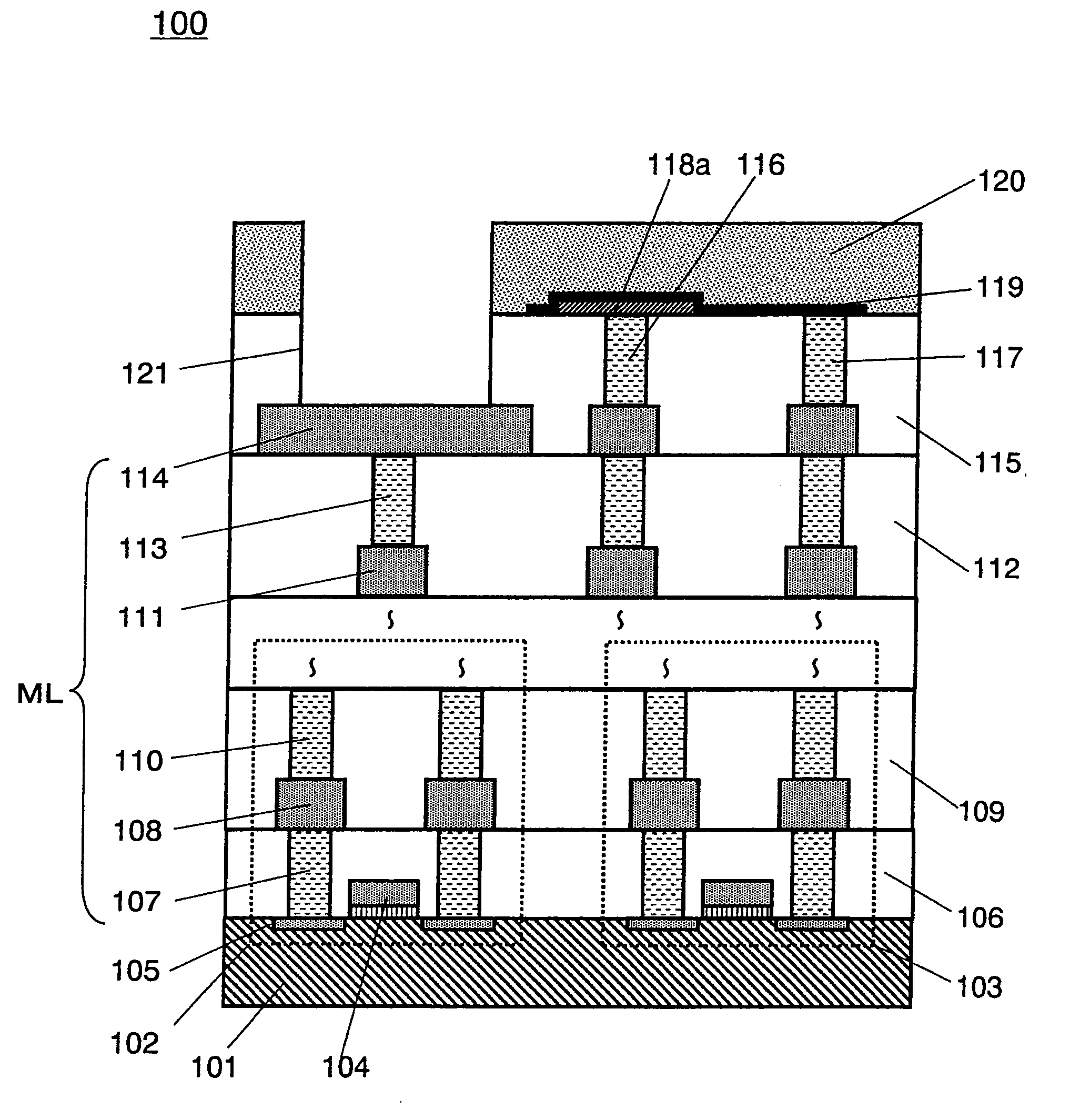
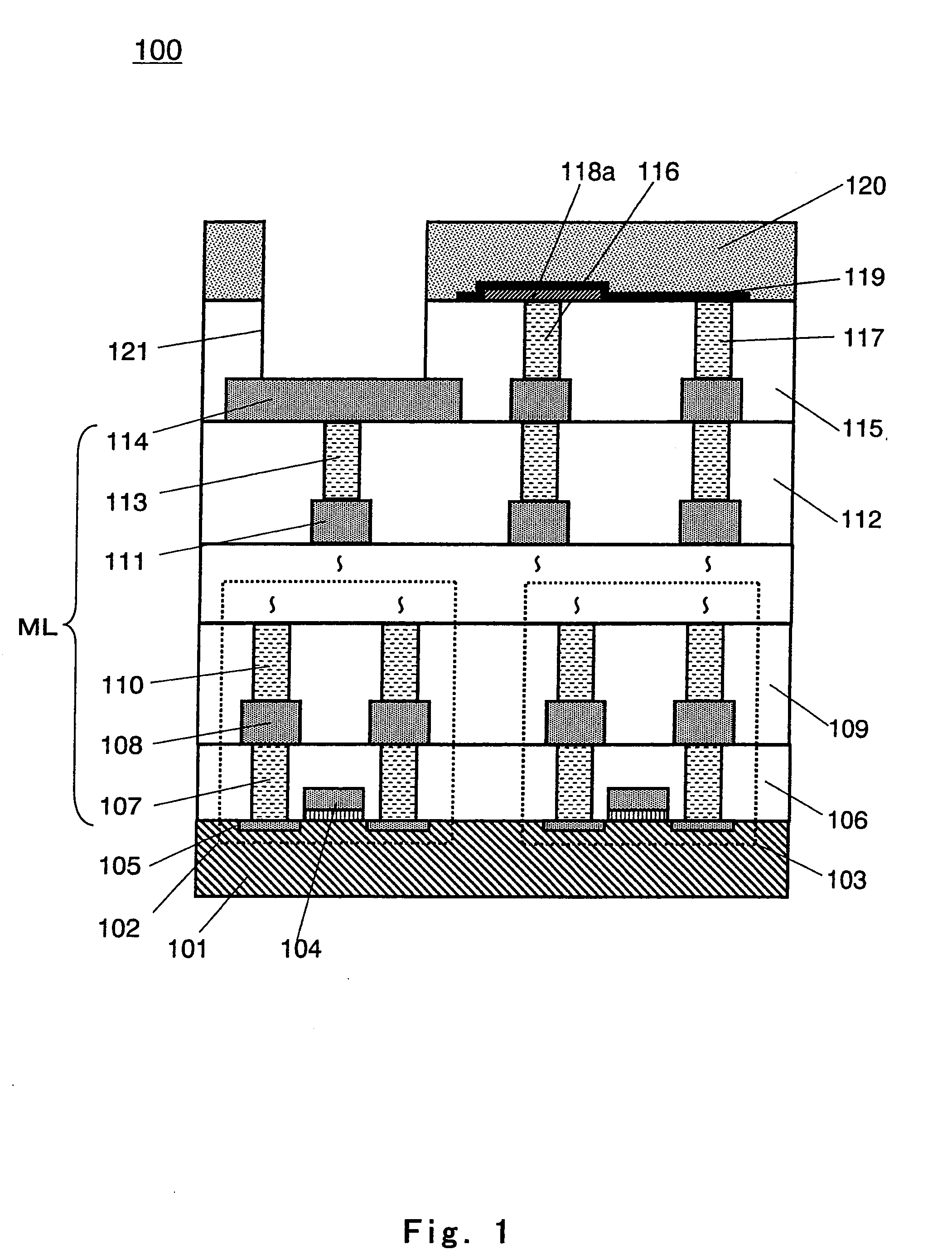
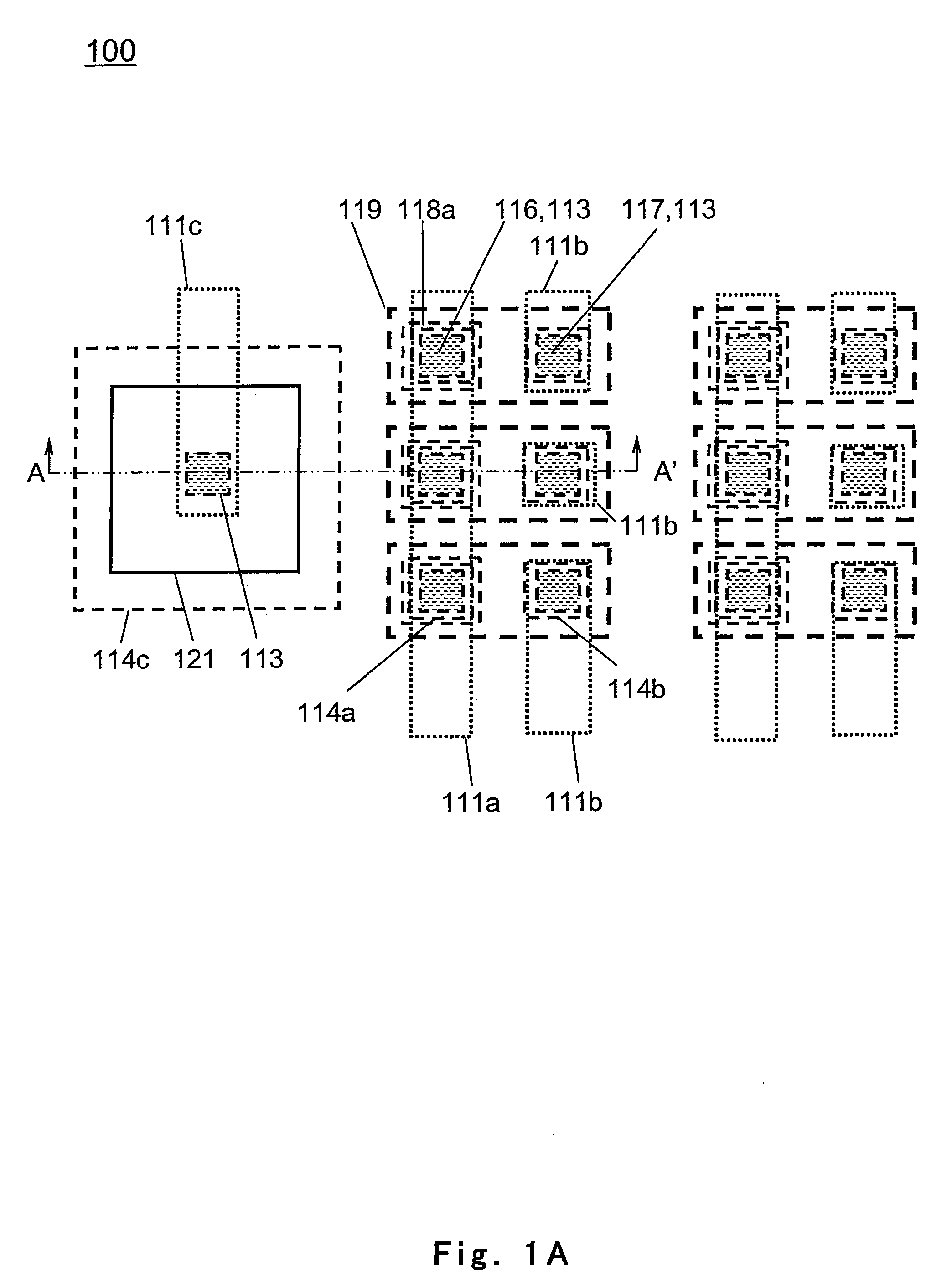
[0071]FIG. 1 is a cross-sectional view showing an exemplary configuration of a semiconductor device 100 according to Embodiment 1 of the present invention.

[0072]As shown in FIG. 1, the semiconductor device 100 of Embodiment 1 includes a substrate 101 provided with a plurality of transistors each including a gate electrode 104 and a diffusion layer 105, a first interlayer insulating layer 106 formed over the substrate 101 to cover the transistors, and a first contact 107 penetrating the first interlayer insulating layer 106 and electrically connected to the diffusion layer 105 of the transistor, resistively. A first wire 108 is formed on the first interlayer insulating layer 106 to cover the first contact 107. A second interlayer insulating layer 109 is formed over the first interlayer insulating layer 106 to cover the first wire 108. A second contact 110 is formed on the first wire 108 and is electrically connected to an upper wire. On the semiconductor substrate 101, a region corre...

embodiment 2

[0103]FIG. 4 is a cross-sectional view showing an exemplary configuration of a semiconductor device 200 according to Embodiment 2 of the present invention.

[0104]As shown in FIG. 4, in the semiconductor device 200 of Embodiment 2, on the uppermost wire 114, the (n+1)-th interlayer insulating layer 115 is formed, and lower electrode 118b of the resistance variable element and the (n+1)-th contact 117 that penetrate the (n+1)-th interlayer insulating layer 115 and are connected to the uppermost wire 114 are formed. The resistance variable layer 119 is formed on the (n+1)-th interlayer insulating layer 115 to cover the lower electrode 118b and the (n+1)-th contact 117. In this case, the lower electrode 118b serves as the first terminal and the (n+1)-th contact 117 serves as the second terminal. Only the passivation layer 120 is formed to directly cover the entire surface (especially, upper surface of the resistance variable element) including the resistance variable element. The pad hol...

embodiment 3

[0116]FIG. 7 is a cross-sectional view showing an exemplary configuration of a semiconductor device 300 according to Embodiment 3 of the present invention.

[0117]As shown in FIG. 7, the semiconductor device 300 of Embodiment 3 has a configuration in which the (n+1)-th interlayer insulating layer 115 is formed between the uppermost wire 114, and the uppermost wire 114 and the (n+1)-th interlayer insulating layer 115 are substantially equal in height from the semiconductor substrate 101, and form a flat surface. The lower electrode 118c of the resistance variable element is formed to be connected to a part of the uppermost wire 114. The resistance variable layer 119 is formed on the (n+1)-th interlayer insulating layer 115 to cover the lower electrode 118c and a part of the uppermost wire. In this case, the lower electrode 118c serves as the first terminal, while the uppermost wire 114 which is at a different electric potential from the lower electrode 118c serves as the second termina...


PUM


Abstract

A semiconductor device (100) of the present invention has a structure in which an interlayer insulating layer (115) is formed on an uppermost wire (114), contacts (116, 117) penetrate the interlayer insulating layer (115), a lower electrode (118a) of the resistance variable element is formed on the interlayer insulating layer (115) to cover the contact (116), and resistance variable layer (119) is formed on the interlayer insulating layer (115) to cover the lower electrode (118a) and the contact (117). The contact (116) and the lower electrode (118a) serve as a first terminal, while the contact (117) serves as a second terminal.

Description

RELATED APPLICATIONS[0001]This application is the U.S. National Phase under 35 U.S.C. §371 of International Application No. PCT / JP2009 / 002570, filed on Jun. 8, 2009, which in turn claims the benefit of Japanese Application No. 2008-151320, filed on Jun. 10, 2008, the disclosures of which Applications are incorporated by reference herein.TECHNICAL FIELD[0002]The present invention relates to a semiconductor device including nonvolatile resistance variable elements which stably change resistance values to be retained, in response to voltage pulses applied, a manufacturing method of the semiconductor device, a semiconductor chip incorporating the semiconductor device, and an application system using the semiconductor device.BACKGROUND ART[0003]In recent years, with advancement of digital technologies, electronic hardware such as portable information devices and information home appliance have been developed to provide higher speeds and higher functionalities. With progresses of higher-s...

Claims


Application Information

Patent Timeline
Patent Type & Authority Applications(United States)
IPC IPC(8): H01H85/00H01L45/00H01L21/02
CPCG11C13/0007G11C2213/32H01L27/24H01L27/101G11C2213/34H10B63/00
Inventor MIKAWA, TAKUMISHIMAKAWA, KAZUHIKO
Owner SYMANTEC CORP
Why Eureka
Try Eureka