

Touch sensor, display and electronic unit
a technology of touch sensor and electronic unit, applied in the field of display, can solve the problems of limited design flexibility, realistically difficult to apply the liquid crystal display elements with the touch sensor to mobile devices, limited conductive film arrangement of touch sensor, etc., and achieves the effect of easy separation, and less influence of external nois
- Summary
- Abstract
- Description
- Claims
- Application Information
AI Technical Summary
Benefits of technology
Problems solved by technology
Method used
Image

Examples
first embodiment
Configuration Example of Display 1
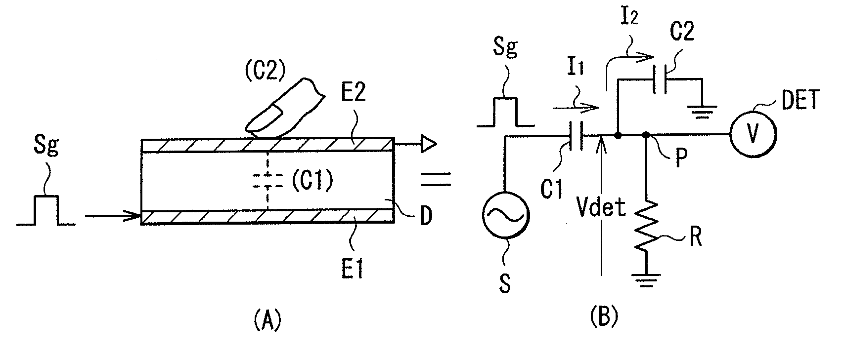
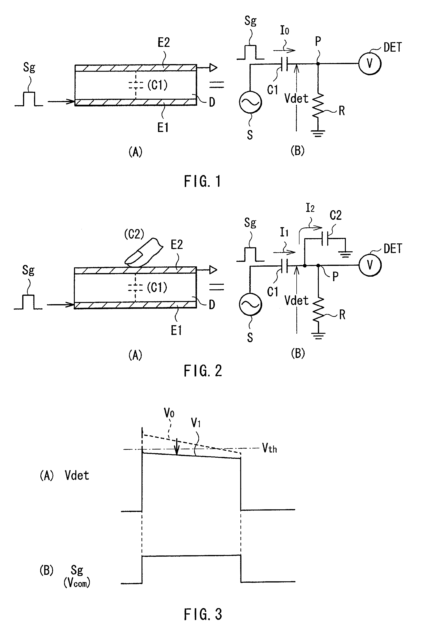
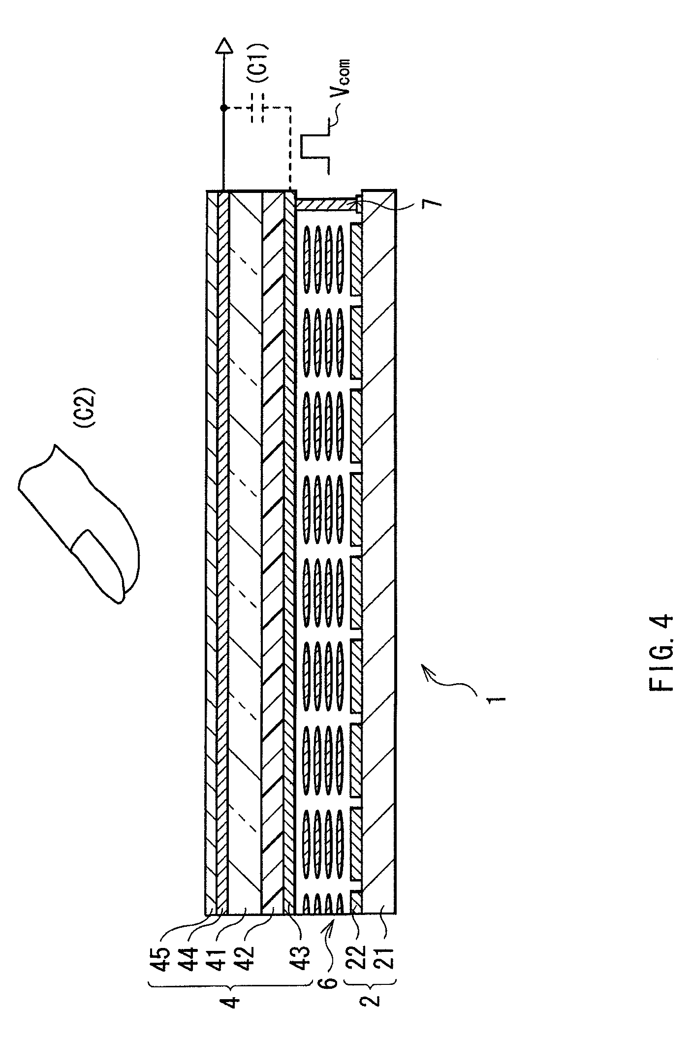
[0060]FIG. 4 illustrates a sectional configuration of a main part of a display 1 with a touch sensor according to a first embodiment of the invention. The display 1 uses a liquid crystal display element as a display element and configures a capacitive type touch sensor by commonly using some (a common electrode 43 which will be described later) of electrodes and a display drive signal (the common drive signal Vcom which will be described later) which are originally included in the liquid crystal display element.
[0061]As illustrated in FIG. 4, the display 1 includes a pixel substrate 2, an opposed substrate 4 arranged to face the pixel substrate 2, and a liquid crystal layer 6 arranged between the pixel substrate 2 and the opposed substrate 4.
[0062]The pixel substrate 2 includes a TFT substrate 21 as a circuit substrate and a plurality of pixel electrodes 22 arranged in a matrix form on the TFT substrate 21. In the TFT substrate 21, in addition to a ...
second embodiment
Modifications of Second Embodiment
[0170]In addition, in the embodiment, the sensor detection electrode 44 is arranged on a surface (on a side opposite to a side facing the liquid crystal layer 6) of the glass substrate 41, but the arrangement of the sensor detection electrode 44 may be modified as follows.
[0171]For example, as in the case of a display 1C illustrated in FIG. 21, in an opposed substrate 4C, the sensor detection electrode 44 may be arranged closer to the liquid crystal layer 6 than the color filter 42.
[0172]Alternatively, as in the case of a display 1D illustrated in FIG. 22, in an opposed substrate 4D, the sensor detection electrode 44 may be arranged between the glass substrate 41 and the color filter 42. In this case, in the case of the transverse electric mode, when electrodes are arranged in a longitudinal direction, an electric field is applied in the longitudinal direction, and liquid crystal molecules rise, thereby to cause large degradation in viewing angle or...
application examples
[0173]Next, referring to FIG. 23 to FIGS. 27A to 27G, application examples of the display with the touch sensor described in the above-described embodiments and the above-described modifications will be described below. The displays according to the above-described embodiments and the like are applicable to electronic units in any fields, such as televisions, digital cameras, notebook personal computers, portable terminal devices such as cellular phones, and video cameras. In other words, the displays according to the above-described embodiments and the like are applicable to electronic units displaying a picture signal inputted from outside or a picture signal produced inside as an image or a picture in any fields.
PUM
 Abstract
Description
Claims
Application Information