Semiconductor Device and Method of Forming Dam Material Around Periphery of Die to Reduce Warpage

Active Publication Date: 2011-02-17
STATS CHIPPAC LTD
View PDF13 Cites 88 Cited by
  • Summary
  • Abstract
  • Description
  • Claims
  • Application Information

AI Technical Summary

Benefits of technology

[0010]A need exists to reduce warpage in a FO-WLCSP during the manufacturing process. Accordingly, in one embodiment, the present invention is a method of making a semiconductor device comprising the steps of providing a temporary carrier having a designated area for a first semiconductor die, depositing dam material on the temporary carrier around the designated area for a first semiconductor die, mounting the first semiconductor die with its active surface oriente

Problems solved by technology

A common failure issue for the FO-WLCSP is warpage.
When the semiconductor die is mounted to a temporary carrier for encapsulation, a mismatch between the coefficient of thermal expansion (CTE) of the encapsulant and temporary carrier induces stress tha

Method used


Image

  • Semiconductor Device and Method of Forming Dam Material Around Periphery of Die to Reduce Warpage
  • Semiconductor Device and Method of Forming Dam Material Around Periphery of Die to Reduce Warpage
  • Semiconductor Device and Method of Forming Dam Material Around Periphery of Die to Reduce Warpage

Examples


Example

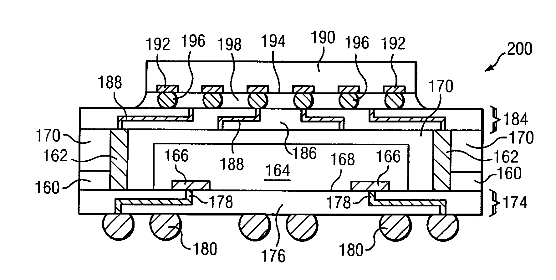
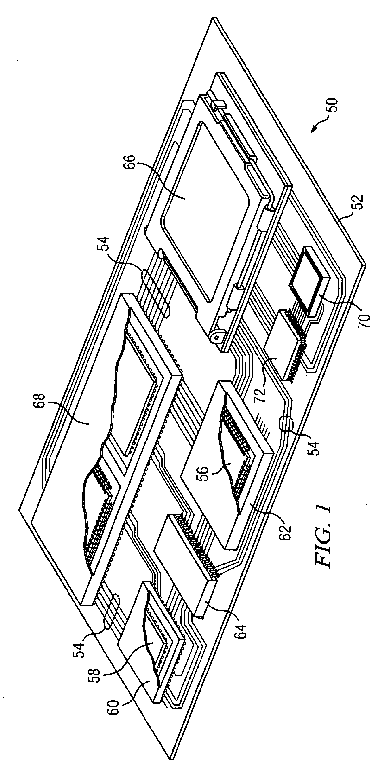
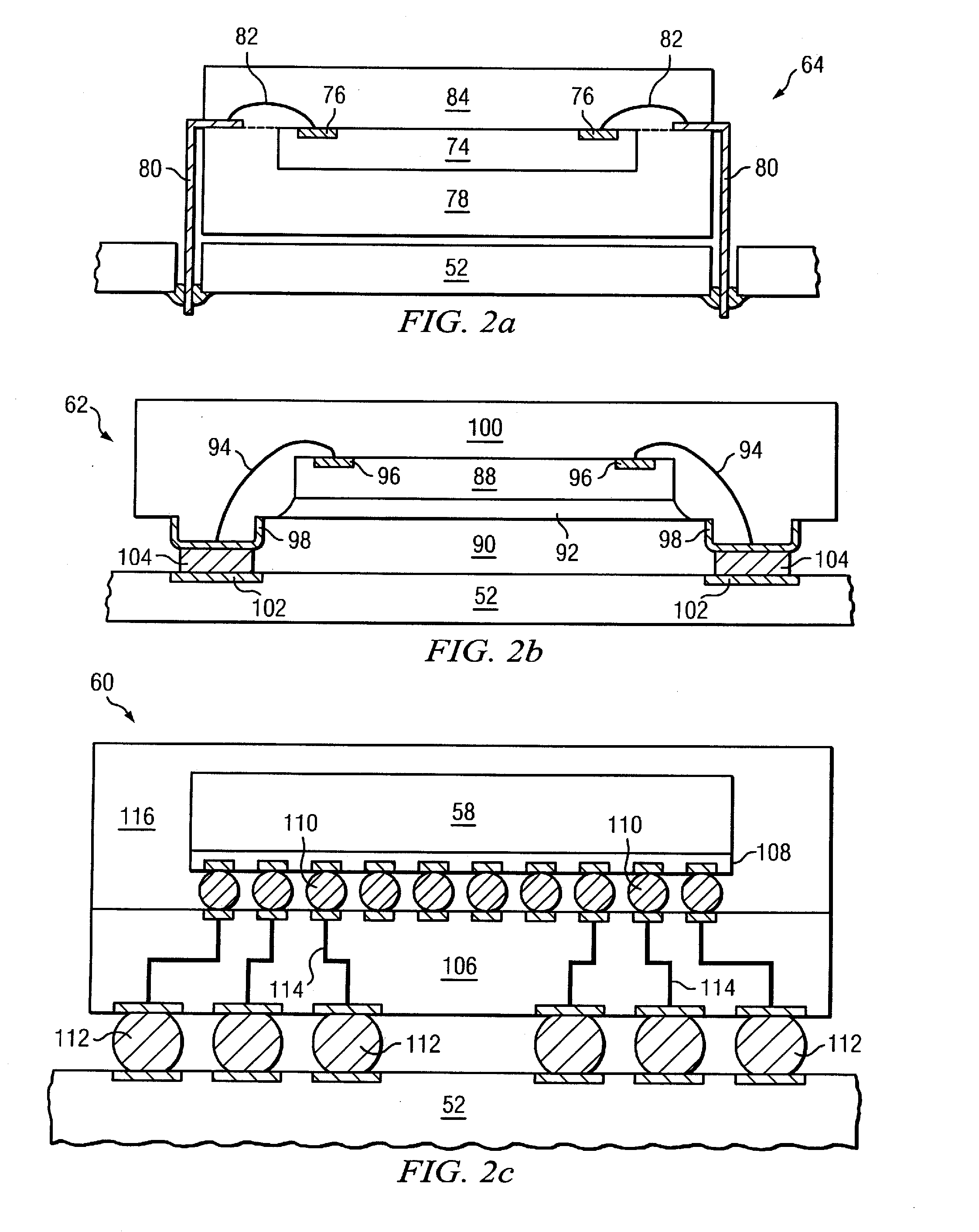
DETAILED DESCRIPTION OF THE DRAWINGS

[0023]The present invention is described in one or more embodiments in the following description with reference to the figures, in which like numerals represent the same or similar elements. While the invention is described in terms of the best mode for achieving the invention's objectives, it will be appreciated by those skilled in the art that it is intended to cover alternatives, modifications, and equivalents as may be included within the spirit and scope of the invention as defined by the appended claims and their equivalents as supported by the following disclosure and drawings.

[0024]Semiconductor devices are generally manufactured using two complex manufacturing processes: front-end manufacturing and back-end manufacturing. Front-end manufacturing involves the formation of a plurality of die on the surface of a semiconductor wafer. Each die on the wafer contains active and passive electrical components, which are electrically connected to ...


PUM


Abstract

A semiconductor device has a temporary carrier with a designated area for a first semiconductor die. A dam material is deposited on the carrier around the designated area for a first semiconductor die. The first semiconductor die is mounted to the designated area on the carrier. An encapsulant is deposited over the first semiconductor die and carrier. The dam material is selected to have a CTE that is equal to or less than the CTE of the encapsulant. The carrier is removed to expose the encapsulant and first semiconductor die. A first interconnect structure is formed over the encapsulant. An EMI shielding layer can be formed over the first semiconductor die. A second interconnect structure is formed over a back surface of the first semiconductor die. A conductive pillar is formed between the first and second interconnect structures. A second semiconductor die is mounted to the second interconnect structure.

Description

FIELD OF THE INVENTION [0001]The present invention relates in general to semiconductor devices and, more particularly, to a semiconductor device and method of forming dam material around a periphery of a semiconductor die to reduce warpage.BACKGROUND OF THE INVENTION [0002]Semiconductor devices are commonly found in modern electronic products. Semiconductor devices vary in the number and density of electrical components. Discrete semiconductor devices generally contain one type of electrical component, e.g., light emitting diode (LED), small signal transistor, resistor, capacitor, inductor, and power metal oxide semiconductor field effect transistor (MOSFET). Integrated semiconductor devices typically contain hundreds to millions of electrical components. Examples of integrated semiconductor devices include microcontrollers, microprocessors, charged-coupled devices (CCDs), solar cells, and digital micro-mirror devices (DMDs).[0003]Semiconductor devices perform a wide range of functi...

Claims


Application Information

Patent Timeline
IPC IPC(8): H01L23/34H01L21/56
CPCH01L21/561H01L21/565H01L21/6835H01L21/78H01L23/16H01L23/3128H01L23/36H01L23/42H01L23/49816H01L23/49827H01L23/5389H01L23/552H01L23/562H01L24/16H01L24/18H01L24/97H01L25/03H01L25/105H01L25/18H01L2224/04105H01L2224/20H01L2224/48091H01L2224/73265H01L2224/97H01L2924/01002H01L2924/01004H01L2924/01005H01L2924/01013H01L2924/01029H01L2924/0103H01L2924/01033H01L2924/01047H01L2924/01073H01L2924/01074H01L2924/01078H01L2924/01079H01L2924/01082H01L2924/01322H01L2924/09701H01L2924/13091H01L2924/14H01L2924/1433H01L2924/15174H01L2924/15311H01L2924/19041H01L2924/30105H01L2924/3025H01L24/48H01L2224/16225H01L2924/01006H01L2924/014H01L2924/12041H01L2224/0401H01L2924/1306H01L2224/16235H01L2924/00014H01L2224/82H01L2924/00H01L2924/181H01L21/568H01L24/19H01L24/96H01L2224/12105H01L2224/32245H01L2224/73267H01L2924/3511H01L2224/05111H01L2224/05124H01L2224/05139H01L2224/05144H01L2224/05147H01L2224/05155H01L2224/05611H01L2224/05624H01L2224/05639H01L2224/05644H01L2224/05647H01L2224/05655H01L2924/00012H01L2224/45099H01L2224/45015H01L2924/207
Inventor PAGAILA, REZA A.
Owner STATS CHIPPAC LTD
Why Eureka
Try Eureka