Touch screen panel and fabrication method thereof

a technology of touch screen and fabrication method, applied in the field of touch screen panel, can solve the problems of weak against static electricity applied from the outside, overlapped area between, etc., and achieve the effects of reducing or minimizing the light emission area, improving visibility, and improving the ability of coupling pattern to resis

Active Publication Date: 2011-03-03
SAMSUNG DISPLAY CO LTD
View PDF17 Cites 64 Cited by
  • Summary
  • Abstract
  • Description
  • Claims
  • Application Information

AI Technical Summary

Benefits of technology

[0016]An aspect of an embodiment of the present invention relates to a touch screen panel in which first sense cells and second sense cells formed on a same layer and coupling patterns that couple adjacent ones of the first sense cells and adjacent ones of the second sense cells to each other, respectively, are constituted of a same material as a metal pattern located on a peripheral region of a touch screen panel. The coupling patterns are crossing with each other, thereby improving the ability of the coupling patterns to withstand static electricity, and a fabrication method thereof.
[0017]In addition, an aspect of an embodiment of the present invention relates to a touch screen panel in which a dummy line comprising a same material as the sense cells is located between the first and second sense cells on a same layer, and the dummy line is electrically coupled to a guard ring formed in an area outside of the display area of the touch screen panel, making it possible to overcome the effects of static electricity applied to the front surface of the touch screen panel as well as the side surface thereof, and a fabrication method thereof.
[0018]Furthermore, an aspect of the present invention relates to a touch screen panel in which when the touch screen panel is formed on an upper substrate constituting a display panel of a flat display panel, it is slantly formed in order to prevent the coupling patterns formed on the touch screen panel from being completely overlapped with the pixels arranged in a stripe shape, making it possible to improve visibility, and a fabrication method thereof.
[0032]With the embodiments as described above, the coupling patterns that couple adjacent ones of the first sense cells and adjacent ones of the second sense cells, respectively, may be implemented with the metal material having a low resistance value as the metal pattern formed in a peripheral region of the touch screen panel, and the coupling patterns may not be crossing with each other to improve the ability of the coupling patterns to withstand static electricity, making it possible to solve the problem of electrostatic discharge (ESD).
[0033]Moreover, the dummy line formed of the same material as the sense cells may be formed on the area between the first and second sense cells, and the dummy line is coupled electrically to the guard ring formed in the outside of the display area of the touch screen panel, making it possible to overcome the effects of static electricity applied to the front surface of the touch screen panel as well as the side surface thereof.
[0034]Furthermore, when the touch screen panel is formed on the upper substrate constituting the display panel of the flat display panel, the coupling patterns formed on the touch screen panel may be formed slantly at an angle not to be completely overlapped with the pixels arranged on the display area of the display panel in a stripe shape to reduce or minimize the light emission area of the pixels that is blocked by the coupling patterns, making it possible to improve visibility.

Problems solved by technology

However, in this case, the coupling part coupling the second sense patterns is still formed of transparent conductive material with a high resistance value, the overlapped area between the sensing patterns is reduced, and the coupling pattern is positioned on the upper portion of the dielectric layer, having a disadvantage that it is weak against the static electricity applied from the outside.

Method used


Image

  • Touch screen panel and fabrication method thereof
  • Touch screen panel and fabrication method thereof
  • Touch screen panel and fabrication method thereof

Examples


first embodiment

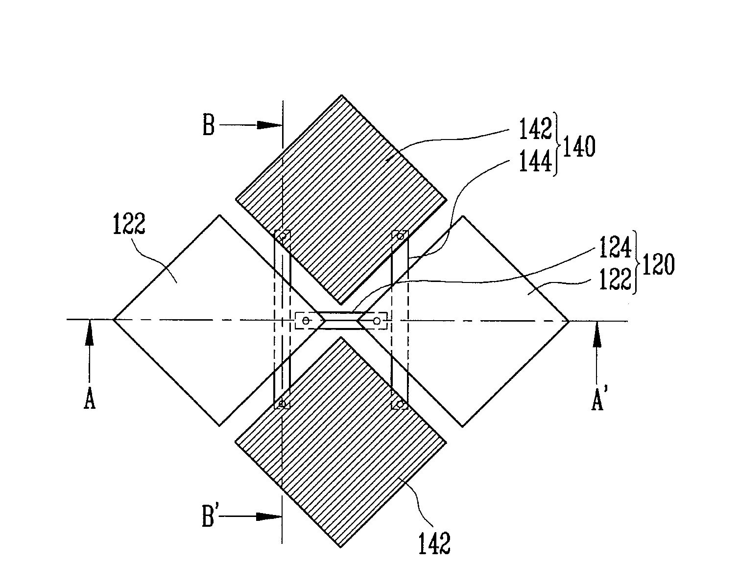
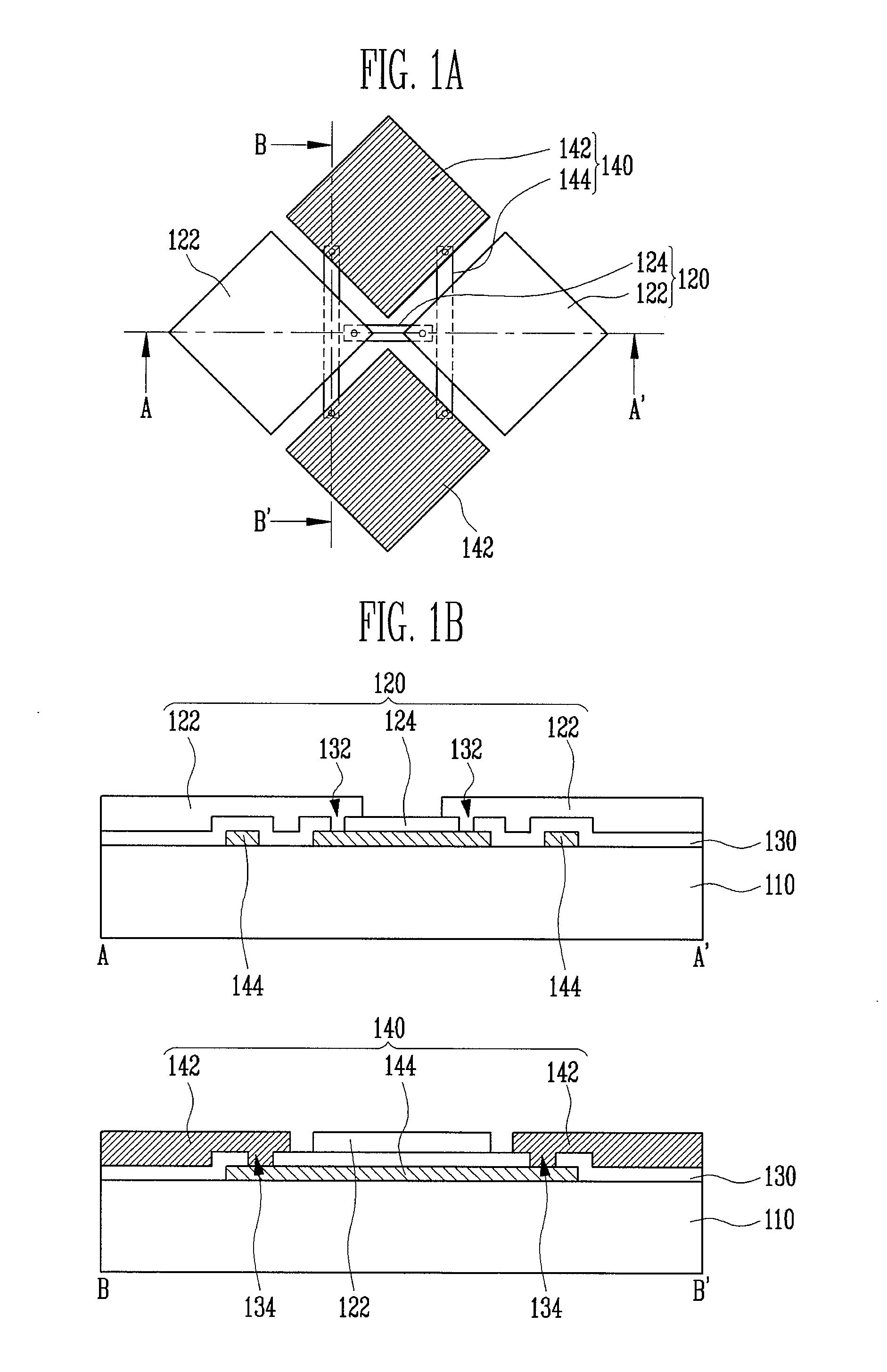
[0045]FIG. 1A is a plan view showing sense patterns on a touch screen panel according the present invention, and FIG. 1B is a cross-sectional view of portions (A-A′ and B-B′) of FIG. 1A.

[0046]Referring to FIGS. 1A and 1B, the sense patterns according to one embodiment of the present invention includes first and second sense patterns 120 and 140 alternately disposed, wherein sense patterns in the same column unit (i.e., having same X coordinate) are coupled to each other, and sense patterns in the same row unit (i.e., having same Y coordinate) are coupled to each other.

[0047]In other words, the first sense patterns 120 include first sense cells 122 arranged in rows extending in a first direction (row direction) and a first coupling pattern 124 for coupling adjacent first sense cells 122 to each other in the same row. The second sense patterns 140 include second sense cells 142 arranged in columns extending in a second direction (column direction) and a second coupling pattern 144 for...

second embodiment

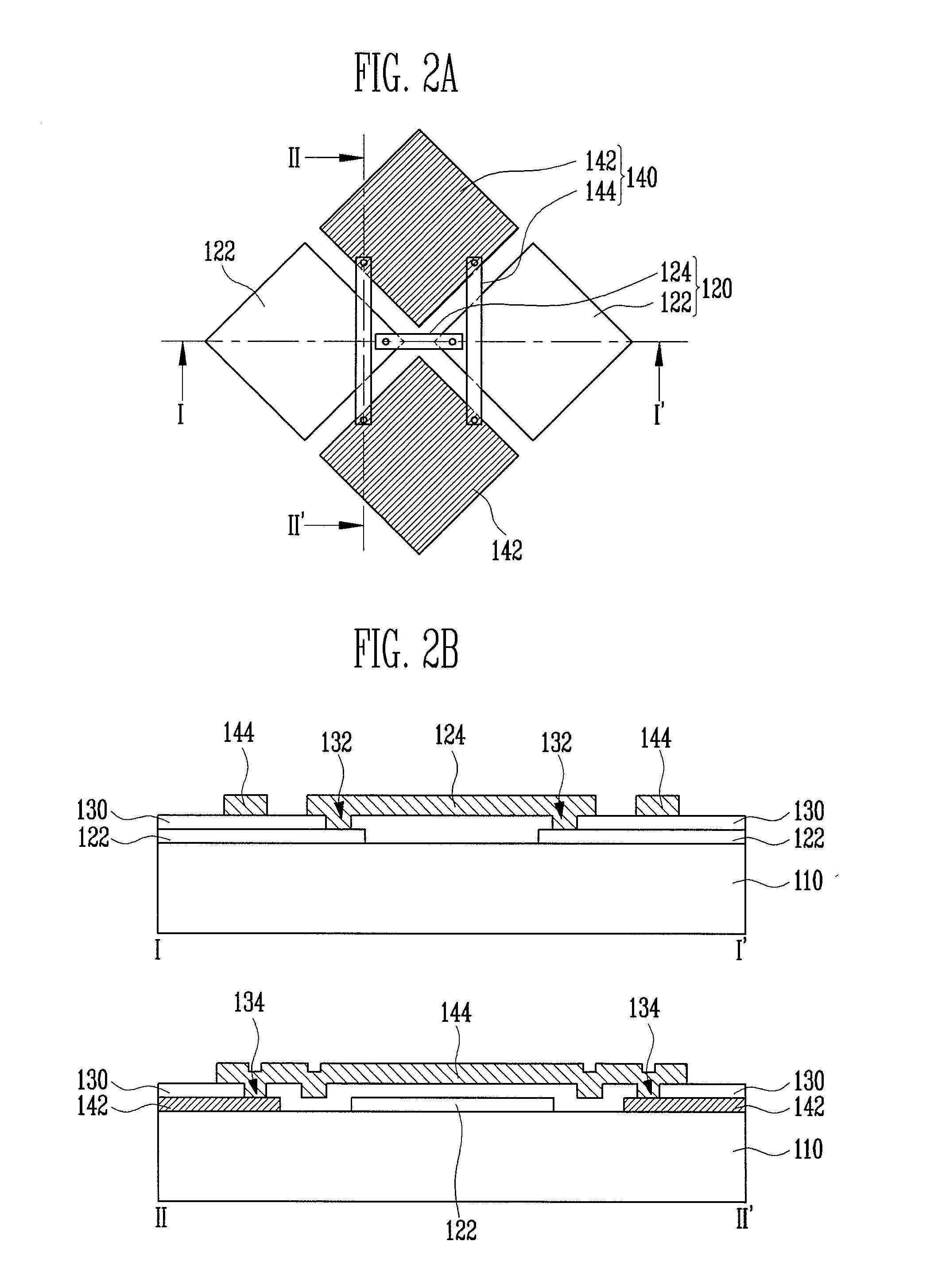
[0063]FIG. 2A is a plan view showing the disposition of sense patterns formed on a touch screen panel according the present invention, and FIG. 2B is a cross-sectional view of portions (I-I′ and II-II') of FIG. 2A.

[0064]In the first embodiment of the present invention as explained through FIG. 1, the first and second coupling patterns 124 and 144 are formed on layers below the first and second sense cells 122 and 142 by way of example, but the present invention is not limited thereto.

[0065]In other words, as shown in FIGS. 2A and 2B, the first and second coupling patterns 124 and 144 may be formed on layers above the first and second sense cells 122 and 142, and in this case, the sense cells 122 and 142 are first formed on a transparent substrate 110, then a dielectric layer 130 in which first and second contact holes 132 and 134 are formed is formed thereon, and the first and second coupling patterns 124 and 144 are formed on the areas on the dielectric layer 130 including the firs...

third embodiment

[0094]FIG. 4 is an exploded plan view of a touch screen panel according to the present invention.

[0095]Compared with the aforementioned first and second embodiments, the third embodiment of the present invention is different therefrom in that a dummy line 170 formed of the same material as the sense cells is formed on the area between the first and second sense cells 122 and 124, and the dummy line 170 is electrically coupled to a guard ring 180 formed at the outside of the display area of the touch screen panel. Therefore, the same reference numerals in the drawings will be used for the same constituents as the first and second embodiments, and the detailed description thereof will be omitted.

[0096]However, for the convenience of explanation, in the third embodiment, the first and second coupling patterns 124 and 144 are formed on layers below the first and second sense cells 122 and 142 by way of example, but the embodiment of the present invention is not limited thereto. In other...


PUM

PropertyMeasurementUnit
refractive indexaaaaaaaaaa
transparentaaaaaaaaaa
resistance valueaaaaaaaaaa

Abstract

A touch screen panel includes first and second sense cells on a same layer and coupling patterns that couple adjacent ones of the first sense cells and adjacent ones of the second sense cells to each other, respectively. The coupling patterns do not cross with each other, thereby improving the ability of the coupling patterns to withstand static electricity. A dummy line formed of a same material as the sense cells may be formed between the first and second sense cells, and the dummy line is electrically coupled to a guard ring located in an area outside of a display area of the touch screen panel, making it possible to overcome the effects of static electricity applied to the front surface of the touch screen panel as well as the side surface thereof.

Description

CROSS-REFERENCE TO RELATED APPLICATIONS[0001]This application claims priority to and the benefit of Korean Patent Application No. 10-2009-0079792, filed on Aug. 27, 2009, in the Korean Intellectual Property Office, the entire content of which is incorporated herein by reference.BACKGROUND[0002]1. Field[0003]An aspect of an embodiment of the present invention relates to a touch screen panel and a fabrication method thereof.[0004]2. Description of Related Art[0005]A touch screen panel is an input device into which a user can input his or her instruction by selecting instruction contents displayed on the screen of an image display device, etc., using a human hand or an object.[0006]To this end, the touch screen panel is provided on the front face of the image display device to convert the contact position directly contacted by the human hand or the object into electrical signals. Therefore, the instruction contents selected on the contact position are accepted as input signals. The tou...

Claims


Application Information

Patent Timeline
Patent Type & Authority Applications(United States)
IPC IPC(8): G06F3/041H01H11/00
CPCG06F3/044Y10T29/49105G06F2203/04111G06F3/0443G06F3/0446G06F2203/04107G06F3/0412G06F2203/04103G06F3/0448
Inventor KIM, DO-YOUBKWAK, WON-KYUJANG, BRENT
Owner SAMSUNG DISPLAY CO LTD
Why Eureka
Try Eureka