

Integrated circuit packaging system with encapsulated via and method of manufacture thereof
a technology of integrated circuit and packaging system, which is applied in the direction of electrical apparatus, semiconductor devices, semiconductor/solid-state device details, etc., can solve the problems of high cost, pop design reliability challenges, and long elude the skilled in the art, and achieve the effect of reducing the cost of production
- Summary
- Abstract
- Description
- Claims
- Application Information
AI Technical Summary
Problems solved by technology
Method used
Image

Examples
first embodiment
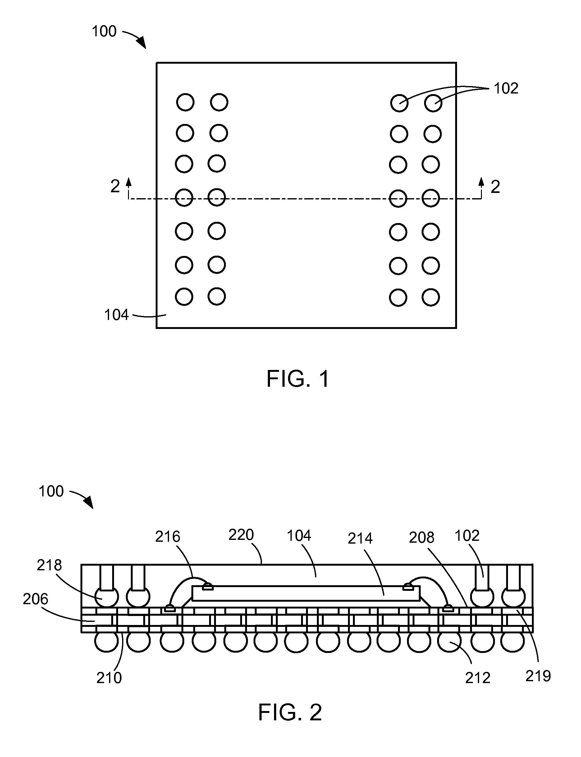
[0026]Referring now to FIG. 1, therein is shown a top view of an integrated circuit packaging system 100 in the present invention. The top view depicts vias 102, such as conductive channels or conductive plugs, along the periphery of an encapsulation 104, such as an encapsulation formed from an epoxy molding compound, a penetrable encapsulation material, or a wire in film.
[0027]For illustrative purposes, the integrated circuit packaging system 100 is shown with the vias 102 along the peripheral portion of the encapsulation 104, although it is understood that the integrated circuit packaging system 100 can have a different configuration for the vias 102. For example, the vias 102 may be placed towards or at a central portion of the encapsulation 104 or along all the sides of the integrated circuit packaging system 100.
[0028]The vias 102 can be formed in a number of different ways. For example, the vias 102 can be formed by a via formation process (not shown) such as laser-ablating or...
second embodiment
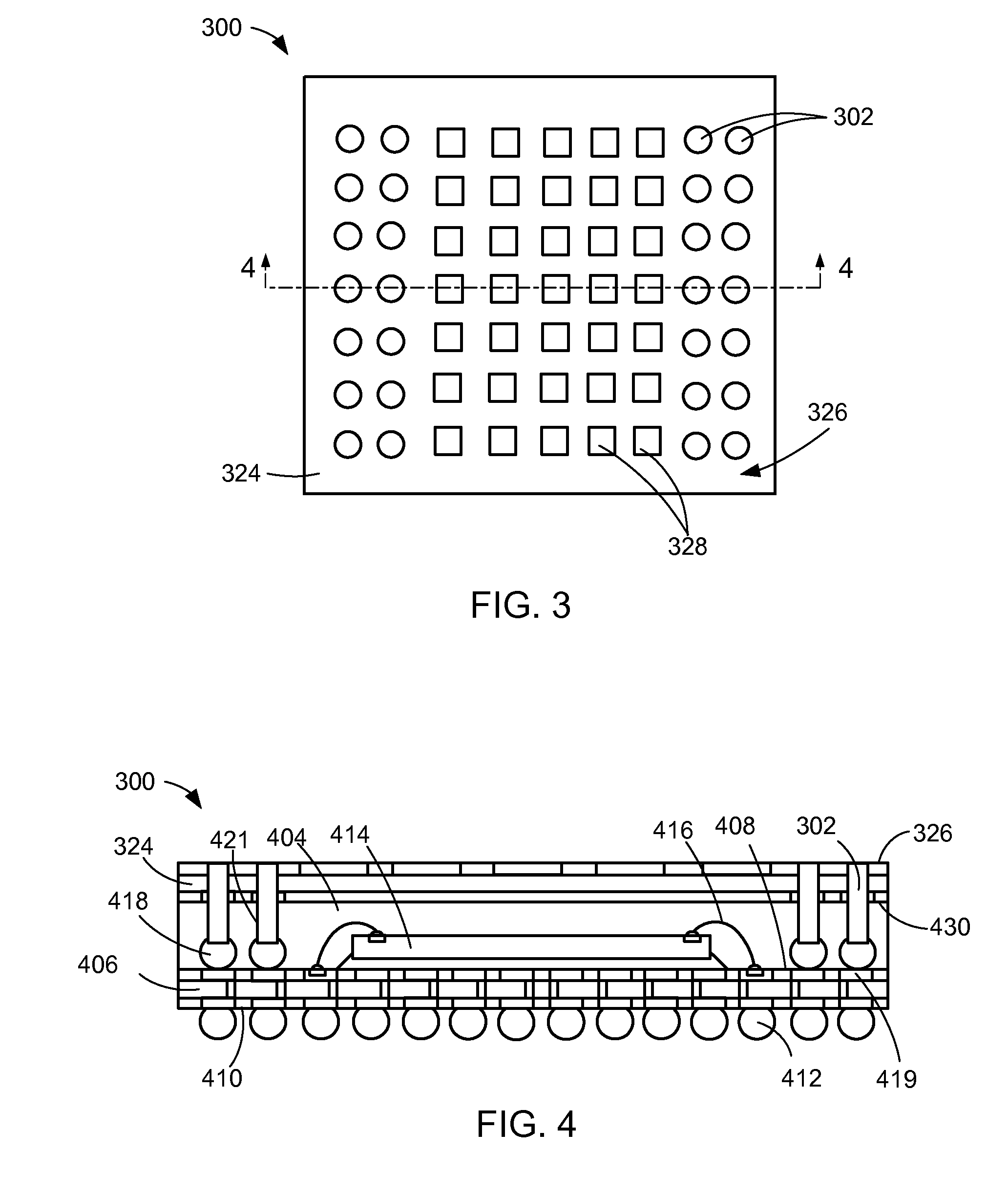
[0039]Referring now to FIG. 3, therein is shown a top view of an integrated circuit packaging system 300 in the present invention. The top view depicts an interposer 324, such as a strip or segment based laminate, a tape, or a lead frame. The interposer 324 includes an interposer first side 326. Mounting pads 328, such as contact pads or terminal pads, can be exposed from the interposer first side 326.
[0040]Vias 302, such as conductive channels or conductive plugs, can be exposed from the interposer first side 326 and can be along the periphery of the interposer first side 326. For illustrative purposes, the integrated circuit packaging system 300 is shown with the vias 302 along the peripheral portion of the interposer 324, although it is understood that the vias 302 may not be along the peripheral portion of the interposer 324. For example, the vias 302 may be placed towards or at a central portion of the interposer 324.
[0041]Also for illustrative purposes, the integrated circuit ...
third embodiment
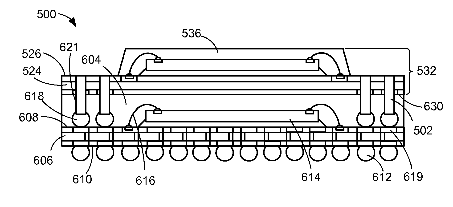
[0051]Referring now to FIG. 5, therein is shown a top view of an integrated circuit packaging system 500 in the present invention. The top view depicts an interstack module 532. The interstack module 532 can include an interposer 524, such as a strip or a segment based laminate, a tape, or a lead frame, having an interposer first side 526. The interstack module 532 can also include a packaged integrated circuit 536, such as an encapsulated integrated circuit die or an encapsulated flip chip, mounted over the interposer first side 526.
[0052]Vias 502, such as conductive channels or conductive plugs, can be exposed from the interposer first side 526 and can be along the periphery of the interposer first side 526. For illustrative purposes, the integrated circuit packaging system 500 is shown with the vias 502 along the peripheral portion of the interposer 524, although it is understood that the vias 502 may not be along the peripheral portion of the interposer 524. For example, the via...
PUM
 Abstract
Description
Claims
Application Information