Unlock instant, AI-driven research and patent intelligence for your innovation.

Thin film transistor array substrate, light-emitting panel and manufacturing method thereof as well as electronic device

a technology of thin film transistors and array substrates, which is applied in the direction of static indicating devices, instruments, solid-state devices, etc., can solve the problems of significant signal delay or voltage drop, increased defective rate, and decreased manufacturing yield

Inactive Publication Date: 2011-03-31
CASIO COMPUTER CO LTD
View PDF3 Cites 21 Cited by
  • Summary
  • Abstract
  • Description
  • Claims
  • Application Information

AI Technical Summary

Benefits of technology

[0013]Advantages of the invention will be set forth in the description which follows, and in part will be obvious from the description, or may be learned by practice of the invention. The advantages of the invention may be realized and obtained by means of the instrumentalities and combinations particularly pointed out hereinafter.

Problems solved by technology

When such a display panel is enhanced in the image quality or increased in the size of its screen, there is a significant signal delay or voltage drop because the length of wirings from a driver varies depending on the location of pixels having light-emitting elements.
Thus, the anode electrode and the cathode electrode cause a short circuit due to the remaining particles, leading to the generation of point defects and decreased manufacturing yield (increased defective rate).

Method used


Image

  • Thin film transistor array substrate, light-emitting panel and manufacturing method thereof as well as electronic device
  • Thin film transistor array substrate, light-emitting panel and manufacturing method thereof as well as electronic device
  • Thin film transistor array substrate, light-emitting panel and manufacturing method thereof as well as electronic device

Examples


Embodiment Construction

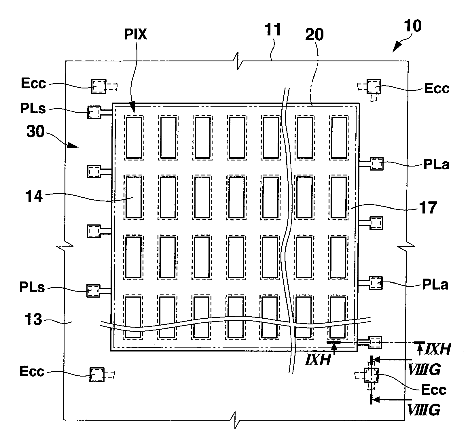
[0030]Hereinafter, a thin film transistor array substrate, a light-emitting panel, and a manufacturing method thereof as well as an electronic device according to an embodiment will be described in detail. First, the light-emitting panel to which the thin film transistor array substrate according to the embodiment is applied and the manufacturing method thereof are described. Here, a display panel in which pixels having organic EL elements are arranged is shown and described as the light-emitting panel to which the thin film transistor array substrate according to the embodiment is applied.

[0031](Light-Emitting Panel)

[0032]FIGS. 1A and 1B are schematic plan views showing an example of the display panel to which the thin film transistor array substrate according to the embodiment is applied. FIG. 1A is a schematic plan view showing a first example of the display panel, and FIG. 1B is a schematic plan view showing a second example of the display panel. FIG. 2 is a schematic plan view ...


PUM


Abstract

A thin film transistor array substrate includes a substrate, thin film transistors formed on the substrate, wirings provided on the substrate. The wirings are subjected to an application of a voltage to drive circuits including the thin film transistors. At least part of the surface of each of the wirings is made of an anodic oxide film.

Description

CROSS-REFERENCE TO RELATED APPLICATIONS[0001]This application is based upon and claims the benefit of priority from prior Japanese Patent Application No. 2009-226156, filed Sep. 30, 2009, the entire contents of which are incorporated herein by reference.BACKGROUND OF THE INVENTION[0002]1. Field of the Invention[0003]The present invention relates to a thin film transistor array substrate.[0004]2. Description of the Related Art[0005]Recently, as a display apparatus for an electronic device such as a mobile telephone or portable music player, there has been known a display apparatus that uses a display panel (light-emitting element type display panel) in which light-emitting elements such as organic electroluminescent elements (hereinafter abbreviated as “organic EL elements”) are two-dimensionally arranged. As compared with a widespread liquid crystal display apparatus, the light-emitting element type display panel to which an active matrix driving method is applied, in particular, ha...

Claims


Application Information

Patent Timeline
IPC IPC(8): G09G5/00H01L33/08
CPCH01L27/3276H01L27/12G09G2300/0861G09G3/3233H01L27/124H10K59/131H10K50/844
Inventor HIGASHI, TOSHIAKI
Owner CASIO COMPUTER CO LTD
Features
  • R&D
  • Intellectual Property
  • Life Sciences
  • Materials
  • Tech Scout
  • Unparalleled Data Quality
  • Higher Quality Content
  • 60% Fewer Hallucinations
Learn More