Stereoscopic liquid crystal display device having touch panel and method for manufacturing the same
- Summary
- Abstract
- Description
- Claims
- Application Information
AI Technical Summary
Benefits of technology
Problems solved by technology
Method used
Image
Examples
first embodiment
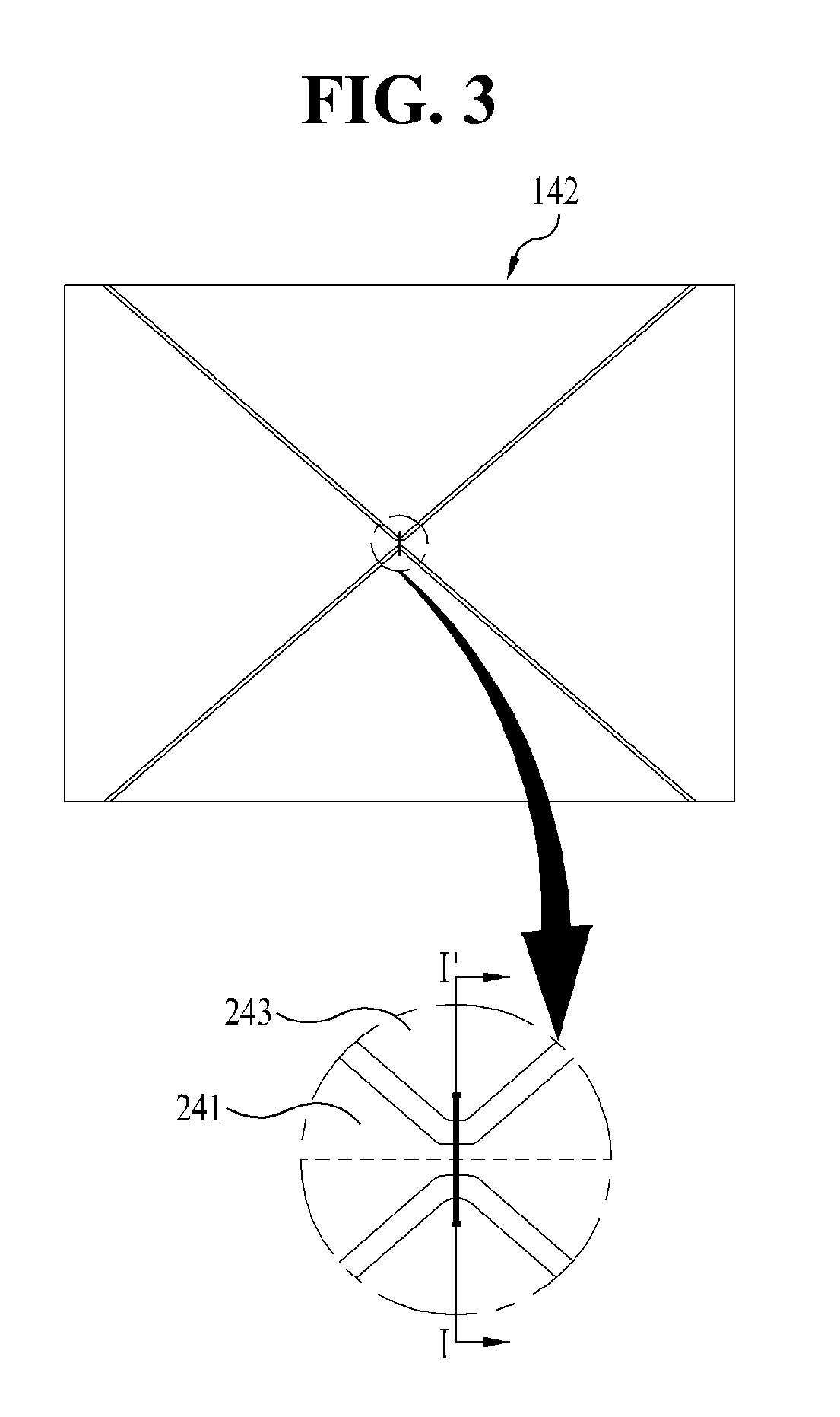
[0055]FIG. 3 illustrates a plane view showing a touch and stereoscopic image lens layer, in a stereoscopic liquid crystal display device having a touch panel according to a first embodiment of the present invention. And, FIG. 4 illustrates a cross-sectional view taken along line I to I′ of FIG. 3.
[0056]Referring to FIG. 3 and FIG. 4, in the stereoscopic liquid crystal display device having a touch panel according to the first embodiment of the present invention, a fourth layer 210 showing a touch function unit of the touch and stereoscopic image lens layer, is provided with a first electrode 243 performing detection in an X-axis and a second electrode 241 performing detection in a Y-axis.
[0057]Herein, the first electrode 243 is electrically connected to a first electrode connecting pattern 211 formed on the lower portion of the touch and stereoscopic image lens layer, through a first contact hole 212a, which is provided in a first insulating layer 212 between the first electrode 243...
second embodiment
[0077]FIG. 6 illustrates a plane view showing a touch and stereoscopic image lens layer in a stereoscopic liquid crystal display device having a touch panel according to a second embodiment of the present invention. And, FIG. 7 illustrates a detailed cross-sectional view of the stereoscopic liquid crystal display device having a touch panel according to the second embodiment of the present invention.
[0078]In comparison with the above-described stereoscopic liquid crystal display device having a touch panel according to the first embodiment of the present invention, in the stereoscopic liquid crystal display device having a touch panel according to the second embodiment of the present invention, the structure of the fourth substrate 210 having the touch function is configured differently, which shown in FIG. 6 and FIG. 7.
[0079]More specifically, referring to FIG. 6 and FIG. 7, the third electrode 251 is formed along the X-axis, first insulating layer 252 is formed on the fourth subst...
PUM
 Abstract
Description
Claims
Application Information


