

Method and system for fracturing a pattern using charged particle beam lithography with multiple exposure passes which expose different surface area
a technology of charged particle beams and lithography, applied in the field of lithography, can solve the problems of high computational cost, difficult to accurately translate the physical design to the actual circuit pattern developed on the resist layer, and difficult to add opc features, so as to reduce the number of shots
- Summary
- Abstract
- Description
- Claims
- Application Information
AI Technical Summary
Benefits of technology
Problems solved by technology
Method used
Image

Examples
Embodiment Construction
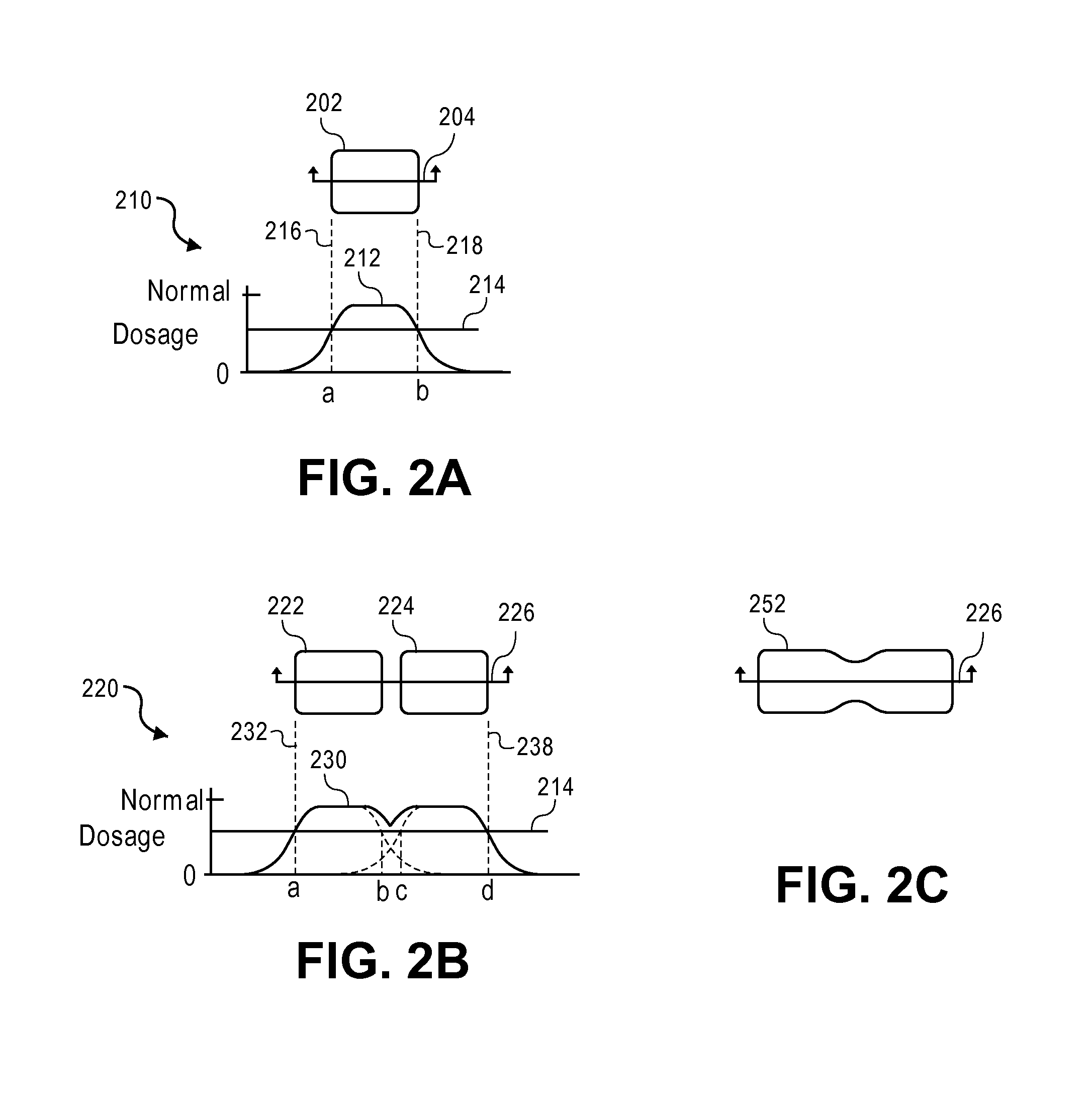
[0043]The present disclosure describes generating and exposing a series of shaped beam charged particle beam shots to form a desired pattern on a surface. The shots are written in multiple exposure passes, wherein any one or more of the following is true:[0044]The base dosage levels of different exposure passes may be different;[0045]The sum of the base dosage levels of all the exposure passes may be different from a normal dosage; or[0046]The union of shot outlines from one exposure pass may be different than the union of shot outlines from a different exposure pass.
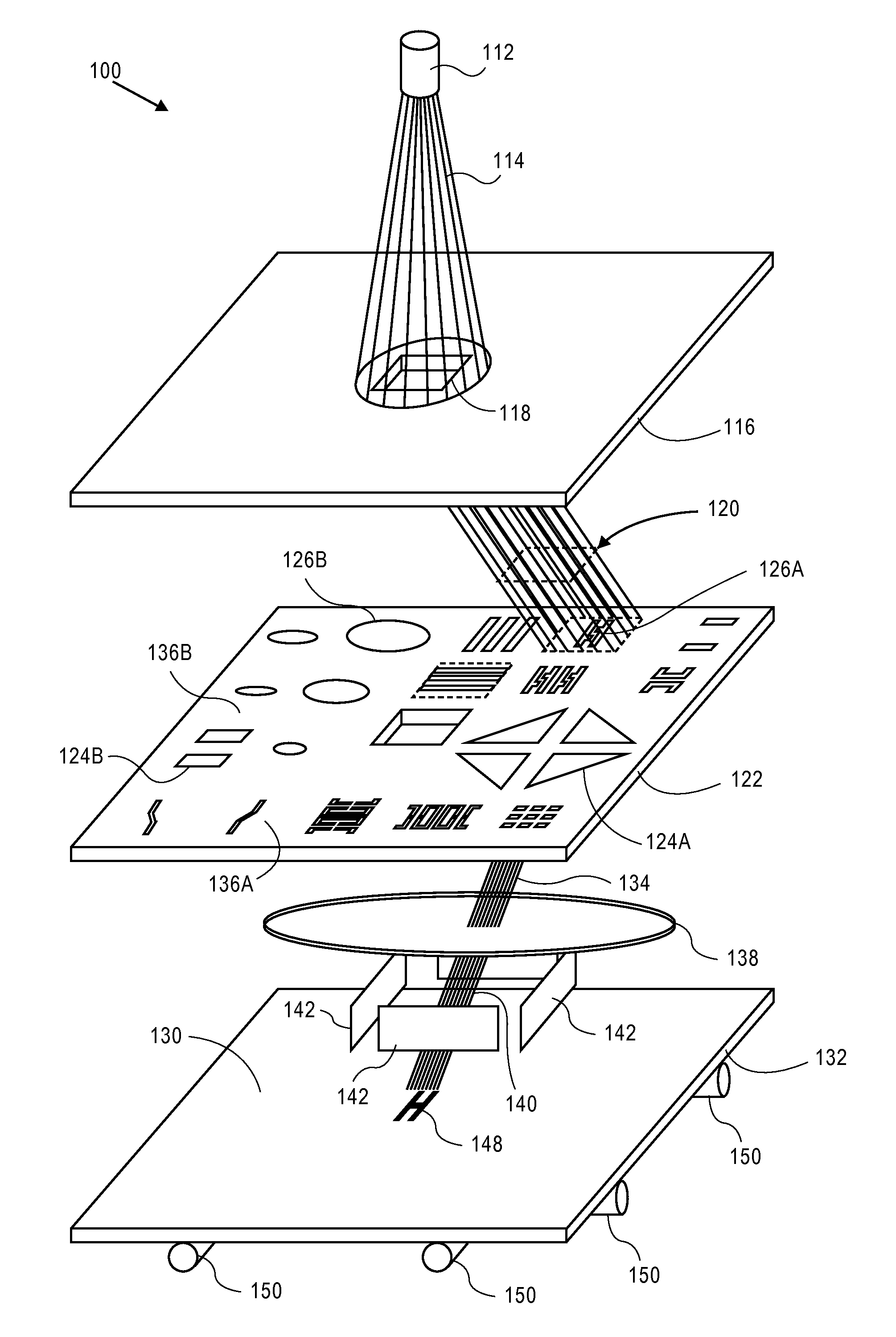
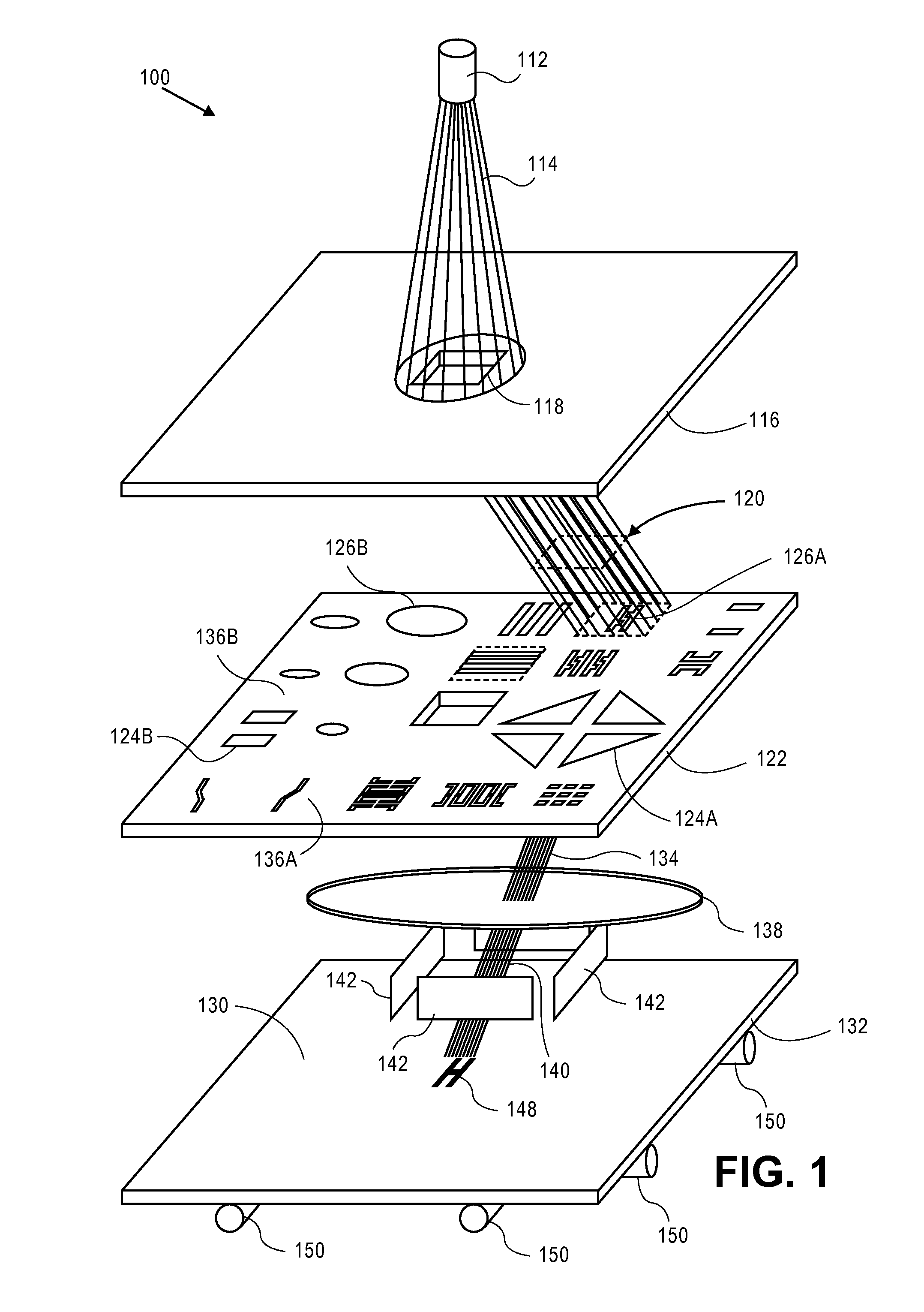
[0047]Referring now to the drawings, wherein like numbers refer to like items, FIG. 1 illustrates an embodiment of a conventional lithography system 100, such as a charged particle beam writer system, in this case an electron beam writer system, that employs character projection to manufacture a surface 130. The electron beam writer system 100 has an electron beam source 112 that projects an electron beam 114 toward an ...
PUM
| Property | Measurement | Unit |
|---|---|---|
| proximity effect | aaaaa | aaaaa |
| area | aaaaa | aaaaa |
| sizes | aaaaa | aaaaa |
Abstract
Description
Claims
Application Information