Liquid crystal display device

a liquid crystal display and display device technology, applied in the direction of identification means, instruments, optics, etc., can solve the problem of processing limits in order to form adhesive sheets

Active Publication Date: 2011-08-18
JAPAN DISPLAY INC +1
View PDF6 Cites 16 Cited by
  • Summary
  • Abstract
  • Description
  • Claims
  • Application Information

AI Technical Summary

Benefits of technology

[0016]According to the invention disclosed in the application, the liquid crystal display device may be provided that is thin as a whole and has a narrow frame area.

Problems solved by technology

However, there is a limit in processing in order to form the adhesive sheet to have a narrow width, and to accurately adhere the adhesive sheet to a corresponding member.

Method used


Image

  • Liquid crystal display device
  • Liquid crystal display device
  • Liquid crystal display device

Examples


first embodiment

[0029]Hereinafter, the invention will be described by referring to the drawings.

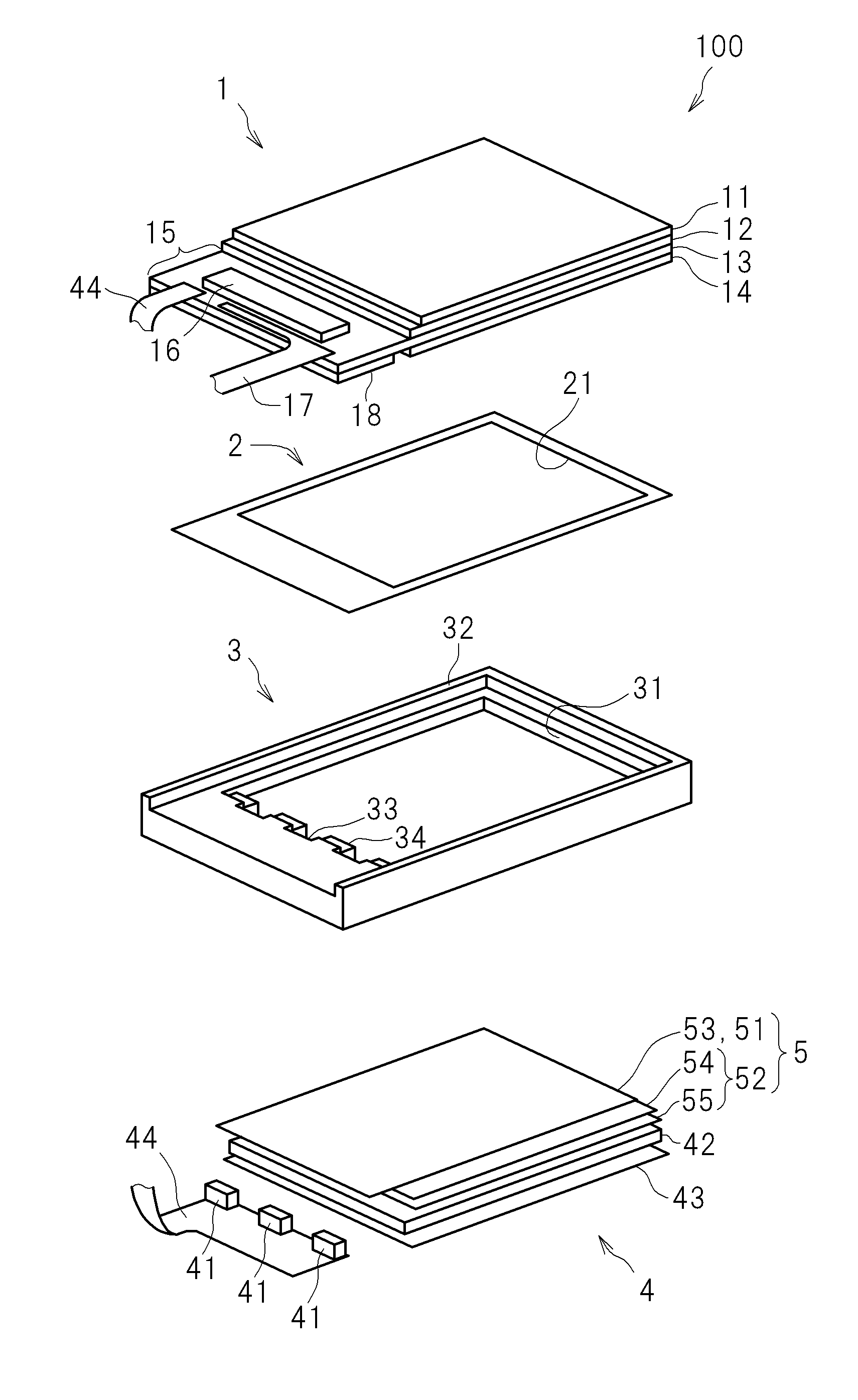
[0030]FIG. 1 is an exploded perspective view illustrating a liquid crystal display device 100 according to the first embodiment of the invention. The liquid crystal display device 100 includes an optical switching member 1, an adhesive sheet 2 which is an adhesive layer, a frame 3, a planar light source 4, and an optical sheet group 5. Further, a user may see an image displayed on the liquid crystal display device 100 from the upside of the same drawing. Hereinafter, the up direction of the same drawing will be referred to as the front surface side, the opposite direction thereof will be referred to as the rear surface side, the surface facing the front surface side will be referred to as the front surface, and the surface facing the opposite side thereof will be referred to as the rear surface.

[0031]An optical switching member 1 has a structure in which a first polarizer 11, a first substrate 12, a seco...

third embodiment

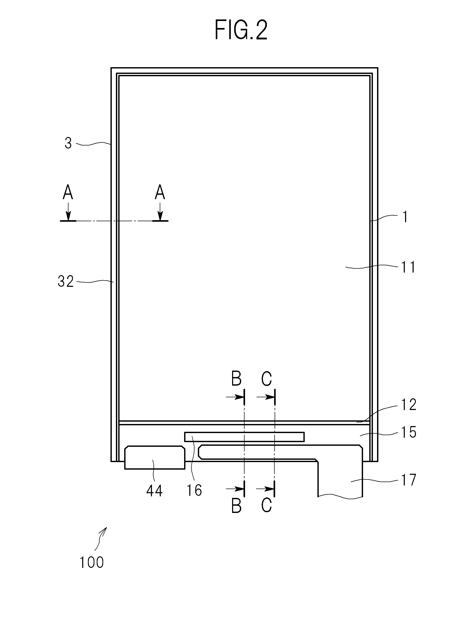
[0060]FIG. 11 is a cross-sectional view taken along the line B-B of FIG. 2 in the The first optical sheet group 351 crosses the front surface side of the LED 41, and extends to a step structure 334 of the frame 3 in the direction of the extension portion 15. Then, the first optical sheet group is interposed between the adhesive sheet 2 and the step structure 334 and is fixed thereto.

[0061]FIG. 12 is a cross-sectional view taken along the line C-C of FIG. 2 in the third embodiment. FIG. 12 is equal to FIG. 11 except that the LEDs 41 are not shown in the drawing.

[0062]As in the liquid crystal display device 300 according to the embodiment, the frame 3 may not be essentially provided with the concave portion. However, when the concave portion 33 is formed as in the first embodiment, the positioning operation of the LEDs 41 may be easily performed during the assembly. Further, the external shape of the expensive first optical sheet group 51 slightly becomes smaller, and the cost involv...


PUM

PropertyMeasurementUnit
thicknessaaaaaaaaaa
thicknessaaaaaaaaaa
thicknessaaaaaaaaaa

Abstract

The liquid crystal display device includes: a substantially rectangular optical switching member in which a first polarizer, a first substrate, a second substrate, and a second polarizer are sequentially provided from a front surface side; a frame which surrounds the optical switching member; a planar light source which is disposed at the rear surface of the optical switching member; at least one optical sheet group which is disposed at the front surface of the planar light source; and an adhesive layer which fixes the optical switching member, the frame, and the optical sheet group to each other, and has a substantially rectangular opening, wherein at least one side of an optical sheet included in the optical sheet group and located at the frontmost surface is adhered to the adhesive layer, and the other sides are located inside the opening of the adhesive layer.

Description

CROSS-REFERENCE TO RELATED APPLICATION[0001]The present application claims priority from Japanese application JP 2010-034110 filed on Feb. 18, 2010, the content of which is hereby incorporated by reference into this application.BACKGROUND OF THE INVENTION[0002]1. Field of the Invention[0003]The present invention relates to a liquid crystal display device.[0004]2. Description of the Related Art[0005]There has been an increasing demand for a decrease in thickness of a small and medium-sized liquid crystal display device used in a portable device, etc. in order to reduce the volume or weight thereof. Here, the small and medium-sized liquid crystal display device has a typical structure in which two polarizers and two glass substrates constituting an optical switching member, and a light guiding plate constituting a planar light source, and plural optical sheets disposed therebetween are stacked, and the stacked structure is fixed to a frame by an adhesive sheet.[0006]JP 2007-163556 A d...

Claims


Application Information

Patent Timeline
Patent Type & Authority Applications(United States)
IPC IPC(8): G02F1/13357
CPCG02F1/133308G02F2202/28G02F1/133305G02F1/133603G02F1/133615G02F1/134363G02F1/1368G02F2001/133607G02F1/133606G02F1/1335G02F1/1333G09F9/00G02F1/133607G02F1/133608G02B6/0091G02F1/133528G02F1/13394G02B6/0051
Inventor OOHIRA, EIJI
Owner JAPAN DISPLAY INC
Why Eureka
Try Eureka