Method and system for approximate placement in electronic designs

a technology of electronic design and placement method, applied in the direction of instruments, computing, electric digital data processing, etc., can solve the problems of inferior placement assignment, inconsistent quality of results, and affecting chip performance, so as to improve runtime, improve performance, and fast and stable placement/floorplanning

Active Publication Date: 2011-09-29
CADENCE DESIGN SYST INC
View PDF14 Cites 17 Cited by
  • Summary
  • Abstract
  • Description
  • Claims
  • Application Information

AI Technical Summary

Benefits of technology

[0010]Thus, a need exists for a method, system, and computer program product for a fast and stable placement / floorplanning method that gives consistent and good quality results. Various embodiments of the present invention provide a method and system for approximate placement of various standard cells, macro-blocks, and I / O pads for the design of integrated circuits by approximating the final shapes of the objects of interest by one or more probability distribution functions over the areas for the objects of interest with improved runtime and very good stability. These probability distributions are gradually localized to final shapes satisfying the placement constraints and optimizing an objective function.
[0011]In some embodiments of the present invention, the aforementioned methods also estimate the final quality of the placement of various standard cells, macro-blocks, and I / O pads. Yet in some other embodiments of the present invention, the aforementioned methods are interleaved with global optimization steps to optimize various objectives according to currently available information and can be naturally combined with the multi-level paradigm. Aside from the advantages of improved runtime and stability, various embodiments of the present invention also allow for incorporating difficult constraints and / or objective functions. Furthermore, although various embodiments of the present invention find their application primarily in electronic design automation, some embodiments of the present invention in other applications where the locations of objects within a specified region or space need to be determined such that the locations optimize some cost functions.

Problems solved by technology

Placement is one of the most fundamental problems in physical design flow since it assigns exact locations for various circuit components within the chip's core area.
An inferior placement of the components may not only affect the chip's performance but also its manufacturability.
For example, inferior placement assignment may produce excessive wirelength which may be beyond the available routing resources.
The quality of the results is, however, inconsistent.
Such force-based or force-directed placement methods seem to give good stability with quality of the results inferior to that of the analytical methods.
The drawback on the force-based methods is that such methods tend to be very slow in reaching the final results.
Although analytic placement methods usually exhibit good stability and give arguably the best quality final results, these methods tend to converge at a much slower speed than the min-cut / partitioning based placement methods or the quadratic programming based methods do.
Otherwise, such a transition is probabilistically rejected.
These simulated annealing methods not only do not significantly improve the netlength, but also tend to reach the final results at an extremely slow speed.
However, partitioning based methods tend to be fast but exhibit low stability and inconsistent quality.
Their quality, however, is generally inferior to that of analytic methods.
Force based placers provide very good stability but are relatively slow and do not work well in the presence of large blocks.
Simulated annealing based placement methods are extremely slow without significantly improving the netlength.
Analytic methods tend to have the best netlength on practical designs but are generally much slower than partitioning or quadratic programming based methods, and the incorporation of different objectives is relatively hard.

Method used


Image

  • Method and system for approximate placement in electronic designs
  • Method and system for approximate placement in electronic designs
  • Method and system for approximate placement in electronic designs

Examples


Embodiment Construction

[0024]Various embodiments of the invention provides a method, system, and computer program product for a fast and stable placement / floorplanning method that give consistent and good quality results.

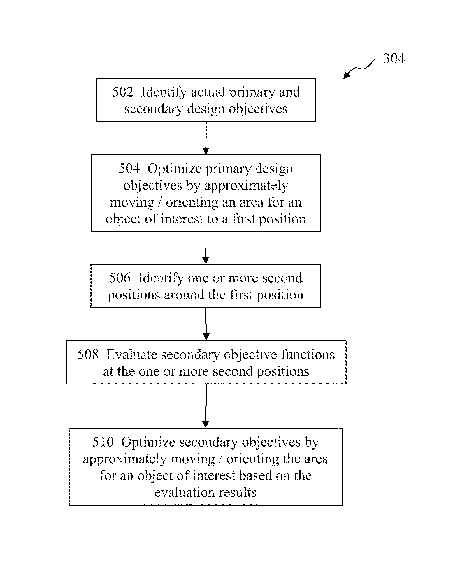
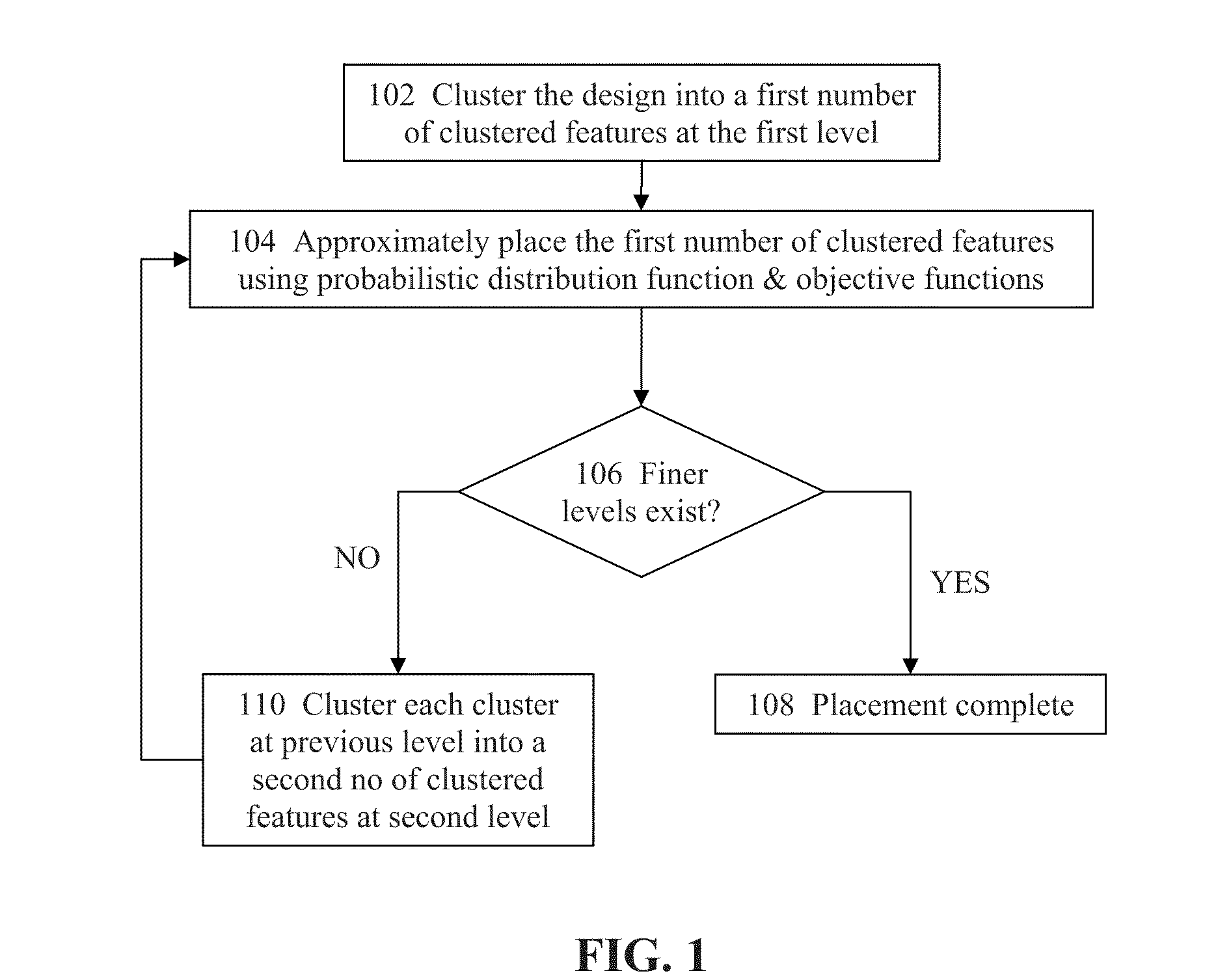
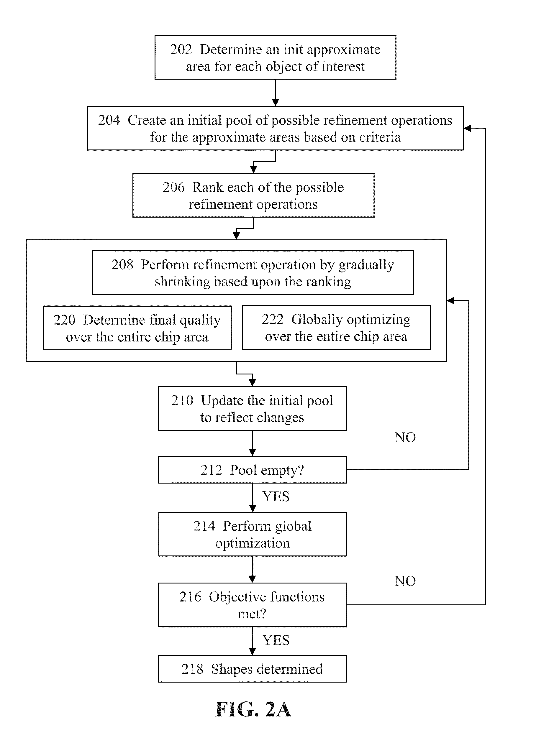
[0025]Various embodiments of the invention provide for a method for approximate placement of objects of interest such as various standard cells, macro-blocks, and I / O pads for the design of integrated circuits by approximating the final shapes (i.e., locations) of the objects of interest by a gradually localized probability distribution function over the chip area with improved runtime and very good stability. In addition to approximating the final result, some embodiments further estimate the final quality of the placement, while some other embodiments further globally optimize placement over the entire chip area. These probability distributions are gradually localized to final feasible shapes satisfying the placement constraints and simultaneously optimizing one or more objective functi...


PUM


Abstract

Disclosed are method, system, and computer program product for a method and system for a fast and stable placement / floorplanning method that gives consistent and good quality results. Various embodiments of the present invention provide a method and system for approximate placement of various standard cells, macro-blocks, and I / O pads for the design of integrated circuits by approximating the final shapes of the objects of interest by one or more probability distribution functions over the areas for the objects of interest with improved runtime and very good stability. These probability distributions are gradually localized to final shapes satisfying the placement constraints and optimizing an objective function.

Description

CROSS REFERENCE TO RELATED APPLICATION(S)[0001]This application constitutes a divisional application of U.S. application Ser. No. 11 / 838,187 filed Aug. 13, 2007 and entitled “METHOD AND SYSTEM FOR APPROXIMATE PLACEMENT IN ELECTRONIC DESIGNS”, the contents of which are hereby expressly incorporated by reference in their entireties.BACKGROUND AND SUMMARY[0002]Placement is one of the most fundamental problems in physical design flow since it assigns exact locations for various circuit components within the chip's core area. An inferior placement of the components may not only affect the chip's performance but also its manufacturability. For example, inferior placement assignment may produce excessive wirelength which may be beyond the available routing resources. As a result, the placer must perform such assignment while optimizing one or more objectives of the circuit to ensure that it meets the design requirements such as wirelength, density, power, timing, and many others.[0003]A pl...

Claims


Application Information

Patent Timeline
Patent Type & Authority Applications(United States)
IPC IPC(8): G06F17/50
CPCG06F17/5072G06F30/392
Inventor CHONG, PHILIPSZEGEDY, CHRISTIAN
Owner CADENCE DESIGN SYST INC
Why Eureka
Try Eureka