

Packaging Process to Create Wettable Lead Flank During Board Assembly
- Summary
- Abstract
- Description
- Claims
- Application Information
AI Technical Summary
Problems solved by technology
Method used
Image

Examples
Embodiment Construction
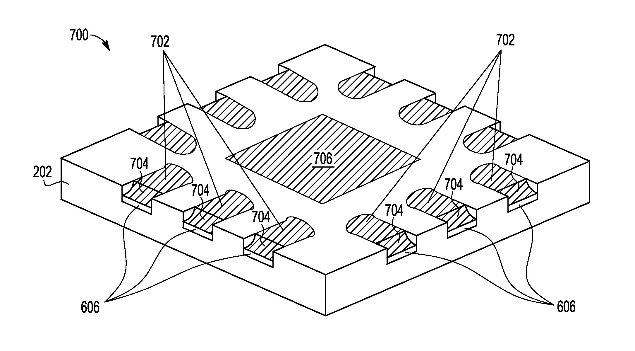
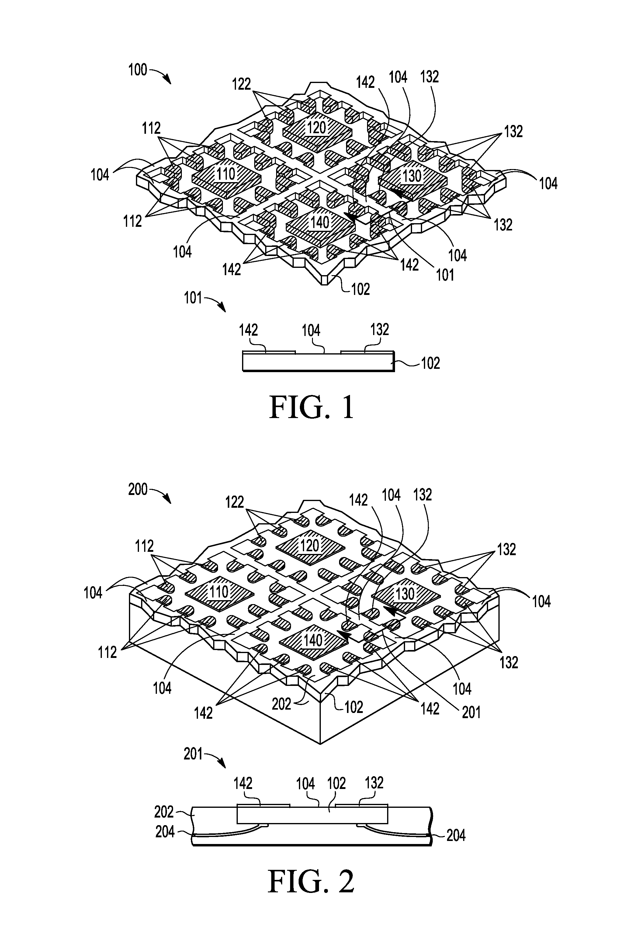
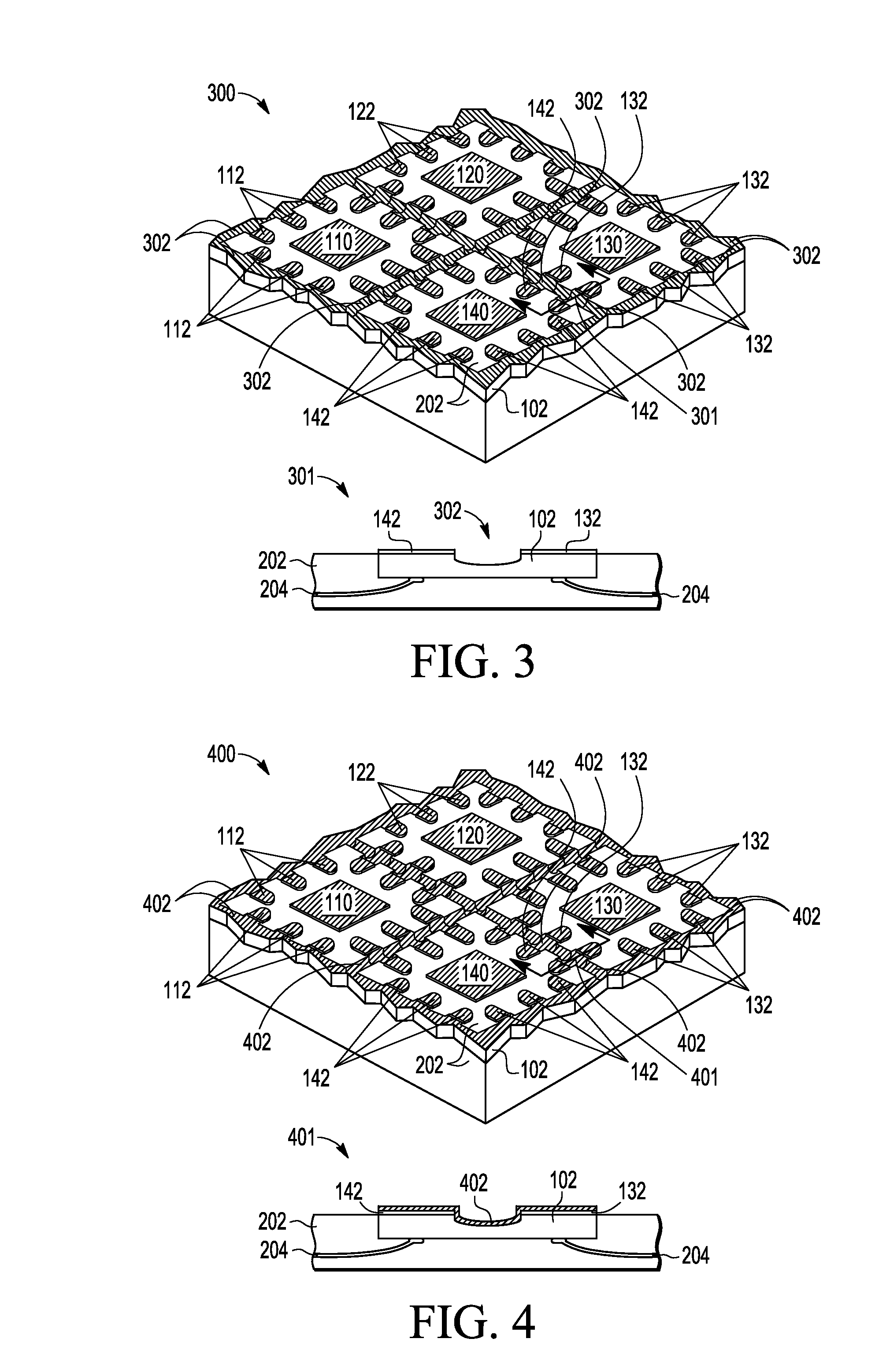
[0015]A method and apparatus are described for fabricating integrated circuit die in lead frame packages (e.g., QFN or PQFN packages) with exposed pad and wettable leads. In selected embodiments, the packaging process begins with a lead frame strip that is selectively plated (e.g., a copper lead frame strip is selectively plated with nickel palladium in the die flag and lead areas). After affixing and wire-bonding the integrated circuit die to the die flags, an encapsulation molding process is then applied to the selectively plated lead frame strip. Subsequently, a selective etch process is applied to partially etch the unplated regions (e.g., copper) on exposed backside surfaces of the lead frame strip to form recesses in the intended singulation areas. Prior to singulation, the recessed areas are then re-plated (e.g., with nickel palladium or any other appropriate wettable material) to a predetermined thickness so that recesses remain in the lead areas, thereby forming wettable le...
PUM
 Abstract
Description
Claims
Application Information