Substrate carrying mechanism, substrate processing apparatus, and semiconductor device manufacturing method

a substrate and carrying mechanism technology, applied in the direction of transportation and packaging, rigid containers, tray containers, etc., can solve the problems of generating scratches and particles, and achieve the effects of reducing the holding force of substrates, stable high-speed carriage, and suppressing the occurrence of scratches and particles

Active Publication Date: 2012-03-15
KOKUSA ELECTRIC CO LTD
View PDF6 Cites 12 Cited by
  • Summary
  • Abstract
  • Description
  • Claims
  • Application Information

AI Technical Summary

Benefits of technology

[0011]According to the above aspects of the present invention, the occurrence of scratches and particles may be suppressed even when deformation has occurred in the substrate, compared to the conventional configuration that supports the substrate only in...

Problems solved by technology

However, in the substrate carrying mechanism described in JP-A No. 2007-184476, in a case when deformation, such as warping and bending, has occurred in the substrate, the substrate contacts at places outside the support portion, a...

Method used


Image

  • Substrate carrying mechanism, substrate processing apparatus, and semiconductor device manufacturing method
  • Substrate carrying mechanism, substrate processing apparatus, and semiconductor device manufacturing method
  • Substrate carrying mechanism, substrate processing apparatus, and semiconductor device manufacturing method

Examples


Embodiment Construction

Exemplary Embodiment

[0025]An exemplary embodiment of the present invention will be described below with reference to the drawings.

(1) Configuration of Substrate Processing Apparatus

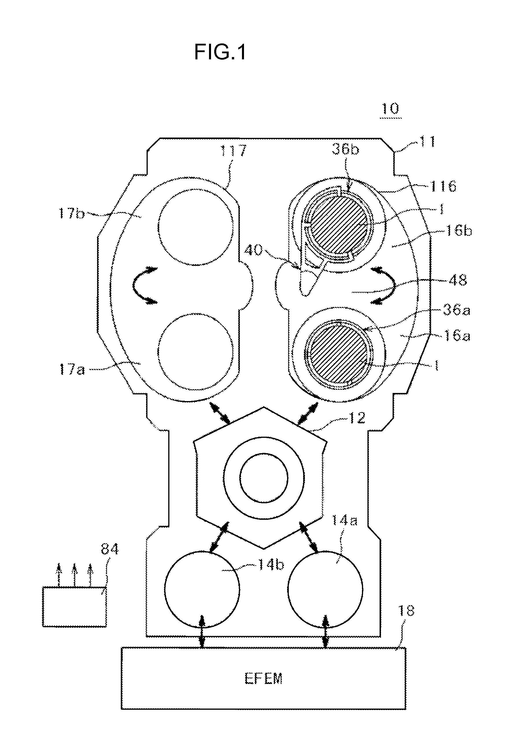
[0026]First, an example configuration of a substrate processing apparatus according to the exemplary embodiment of the present invention will be described. Here, a case where the substrate processing apparatus is an ashing apparatus that performs resist removal will be taken as an example.

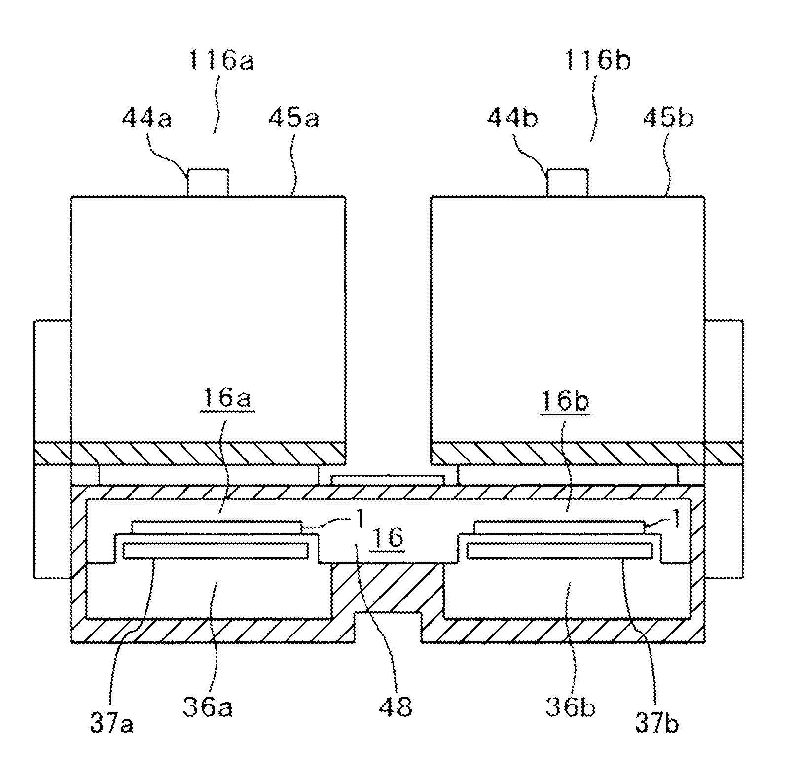
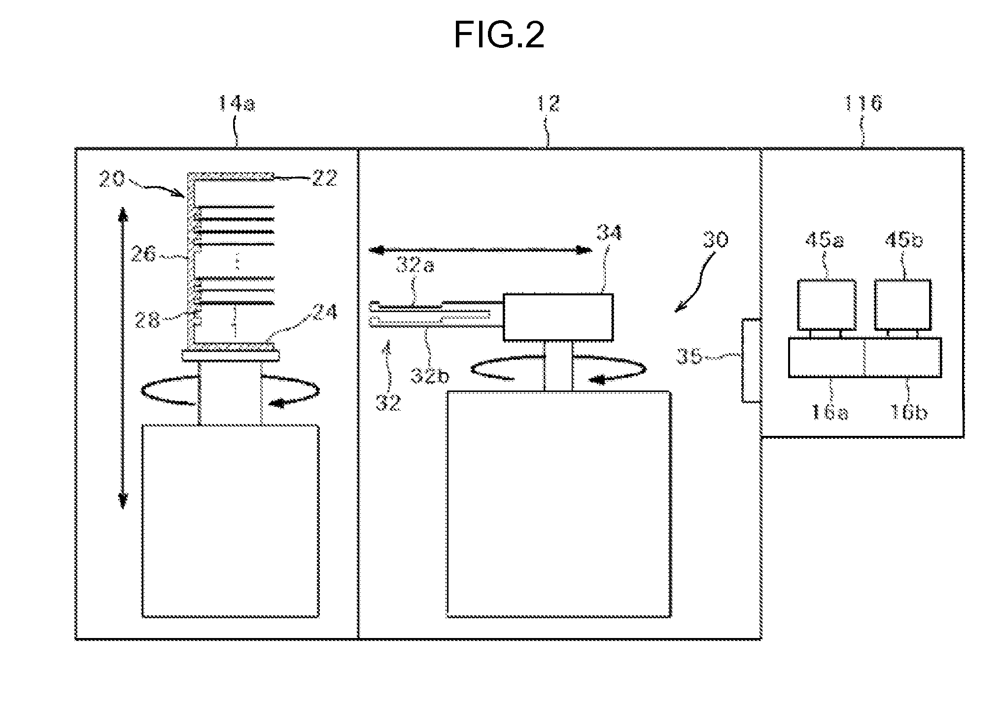
[0027]FIG. 1 is a schematic configuration diagram of a substrate processing apparatus according to the exemplary embodiment of the present invention. FIG. 2 is a vertical sectional view of the substrate processing apparatus shown in FIG. 1. FIG. 3 is a vertical sectional view of the inside of a processing chamber group of the substrate processing apparatus shown in FIG. 1. FIG. 4 is a vertical sectional view of an upper processing chamber and a lower processing chamber of the substrate processing apparatus shown in FIG. ...


PUM

PropertyMeasurementUnit
Diameteraaaaaaaaaa
Areaaaaaaaaaaa

Abstract

The present invention provides a substrate carrying mechanism, a substrate processing apparatus, and a semiconductor device manufacturing method that, when carrying a substrate, suppress the generation of scratches and particles caused by substrate deformation, suppress a decrease in substrate holding force due to substrate deformation, and realizes stable high-speed carriage. Namely, the substrate carrying mechanism, the substrate processing apparatus, and the semiconductor device manufacturing method of the present invention include: a plate-like body that becomes a support base body of a substrate that is a carrying subject; and substrate support portions in which plural convex portions disposed on a surface of the plate-like body are placed on a circumference of a circle that is smaller than the diameter of the substrate.

Description

CROSS-REFERENCE TO RELATED APPLICATION[0001]This application claims priority under 35 USC 119 from Japanese Patent Application No. 2010-206034, filed on Sep. 14, 2010, and No. 2011-133316, filed on Jun. 15, 2011, the disclosures of which are incorporated by reference herein.BACKGROUND OF THE INVENTION[0002]1. Field of the Invention[0003]The present invention relates to a substrate carrying mechanism that supports a substrate that is a carrying subject, a substrate processing apparatus that is equipped with the substrate carrying mechanism, and a semiconductor device manufacturing method that is performed by using the substrate processing apparatus.[0004]2. Description of the Related Art[0005]Generally, substrate processing apparatus used in a semiconductor device manufacturing process are equipped with a processing chamber and a carrying device. The processing chamber processes substrates such as wafers. The carrying device carries the substrates into the processing chamber, and car...

Claims


Application Information

Patent Timeline
IPC IPC(8): H01L21/02B65D1/34H01L21/306
CPCH01L21/68707H01L21/67383H01L21/6875
Inventor TAKAHASHI, AKIRA
Owner KOKUSA ELECTRIC CO LTD
Why Eureka
Try Eureka