Method and System for Optimizing a Device With Current Source Models

a technology of current source model and optimization method, which is applied in the field of device optimization, can solve problems such as time delay in clock signal, and achieve the effect of minimizing clock skew varian

Active Publication Date: 2012-05-17
GLOBALFOUNDRIES US INC
View PDF0 Cites 0 Cited by
  • Summary
  • Abstract
  • Description
  • Claims
  • Application Information

AI Technical Summary

Benefits of technology

[0004]According to one embodiment of the present invention, a method for optimizing a circuit includes at least a first branch and a second branch includes defining an objective function using a shape of waveforms measured at a timing point in each branch, and optimizing the objective function to minimize a variance of clock skew of the first branch and the second branch across different process voltage temperature values.
[0005]According to another embodiment of the present invention, a system for optimizing a circuit includes a memory, and a processor operative to define an objective function using a shape of waveforms measured at a timing point in each branch, and optimize the objective function to minimize a variance of clock skew of the first branch and the second branch across different process voltage temperature values.

Problems solved by technology

For example, the physical length of interconnects between devices in a path, or the properties of a devices in the path may induce a time delay in the clock signal.

Method used


Image

  • Method and System for Optimizing a Device With Current Source Models
  • Method and System for Optimizing a Device With Current Source Models
  • Method and System for Optimizing a Device With Current Source Models

Examples


Embodiment Construction

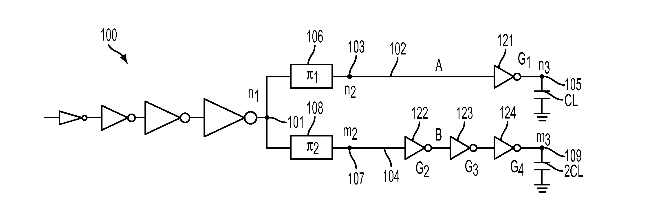
[0014]Clock skew or timing skew is a circuit phenomenon in which the clock signal sent from the clock reference arrives at different components of the circuit at different times. The clock skew can occur for different reasons, such as, for example different electrical properties of the clock signal paths, interconnect lengths, variations in intermediate components of clock branches, PVT conditions, and cross talk. Minimizing the variance of clock skew across different clock paths is a major step in the process of circuit optimization. Furthermore, for the deep submicron technology in which the clock frequency is high, robustness of clock skew is desirable for properly functioning circuits.

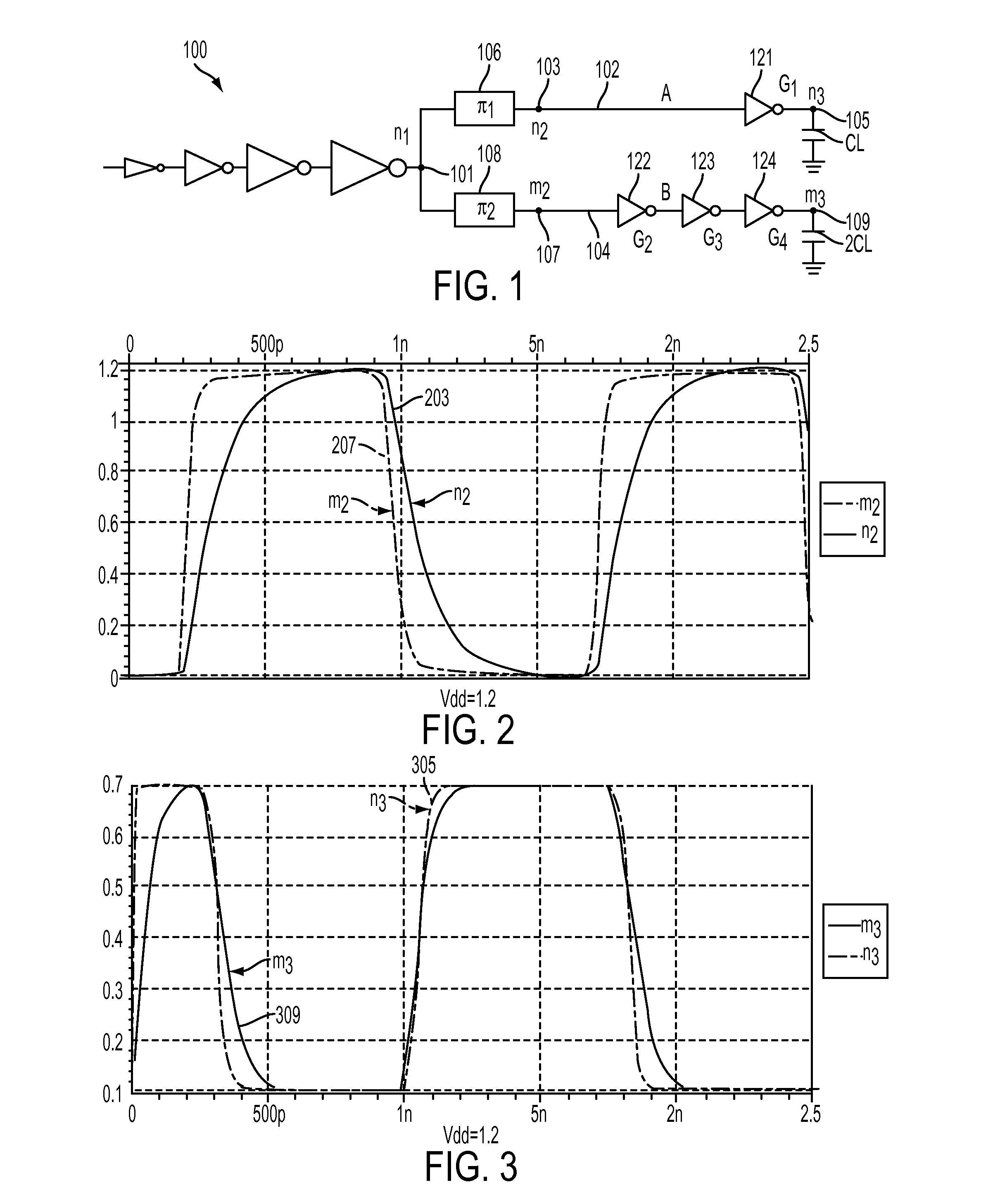
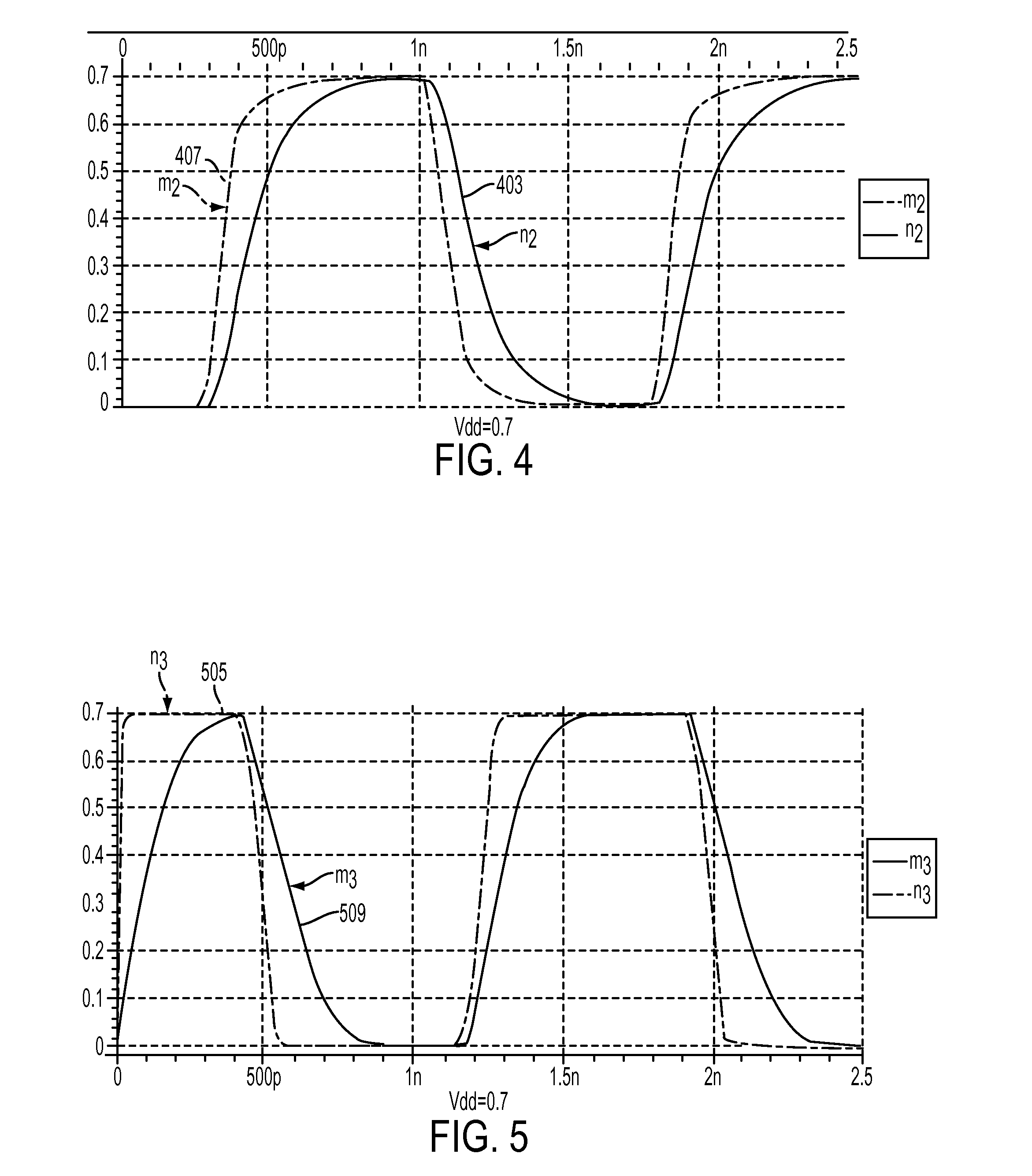
[0015]FIG. 1 illustrates a block diagram of an example of a simulated circuit 100. The circuit 100 includes a node (timing point) n1101 that is connected to a signal path A 102 and a signal path B 104. The signal path A 102 includes nodes n2103 and n3105, and the signal path B 104 includes nodes m2...


PUM


Abstract

A method for optimizing a circuit includes at least a first branch and a second branch includes defining an objective function using a shape of waveforms measured at a timing point in each branch, and optimizing the objective function to minimize a variance of clock skew of the first branch and the second branch across different process voltage temperature values.

Description

BACKGROUND[0001]The present invention relates to device optimization, and more specifically, to minimizing variance of arrival times of waveforms in circuits in the presence of process environmental variations.[0002]Circuit optimization includes, for example, minimizing variance of arrival times of waveforms in circuits in the presence of process voltage temperature variations. Process voltage temperature (PVT) conditions affect the performance of devices in a circuit. For example, changing the temperature of a device in a circuit changes the electrical properties of the device. The time delay of signal paths may be further affected by changes in the PVT conditions.[0003]Many circuits use a system or reference clock to operate effectively. The reference clock outputs a clock signal that may be propagated through a variety of signal paths or branches in a circuit. The signal paths may include conductive interconnects or lines that connect a variety of devices such as field effect tra...

Claims


Application Information

Patent Timeline
Patent Type & Authority Applications(United States)
IPC IPC(8): G06F17/50
CPCG06F17/5031G06F2217/84G06F2217/80G06F30/3312G06F2119/08G06F2119/12
Inventor ABBASPOUR, SOROUSHFELDMANN, PETERHABITZ, PETER A.HATAMI, SAFAR
Owner GLOBALFOUNDRIES US INC
Why Eureka
Try Eureka