Dynamic wafer alignment method in exposure scanner system

a scanning system and dynamic technology, applied in the field of dynamic wafer alignment method in exposure scanning system, can solve the problems of difficult enlargement of the process window of the semiconductor device, and conventional wafer alignment method cannot meet the requirement of high wafer alignment accuracy for the semiconductor device with smaller feature siz

Inactive Publication Date: 2012-06-07
NAN YA TECH
View PDF3 Cites 16 Cited by
  • Summary
  • Abstract
  • Description
  • Claims
  • Application Information

AI Technical Summary

Problems solved by technology

Accordingly, it is difficult to enlarge the process window of the semiconductor devices, especially for wafer alignment accuracy in an exposure equipment during an exposure process and overlay accuracy of the patterns of each layer on the wafer.
Thus, the conventional wafer alignment method cannot satisfy the high wafer alignment accuracy requirement for the semiconductor devices with smaller feature sizes.

Method used


Image

  • Dynamic wafer alignment method in exposure scanner system
  • Dynamic wafer alignment method in exposure scanner system
  • Dynamic wafer alignment method in exposure scanner system

Examples


Embodiment Construction

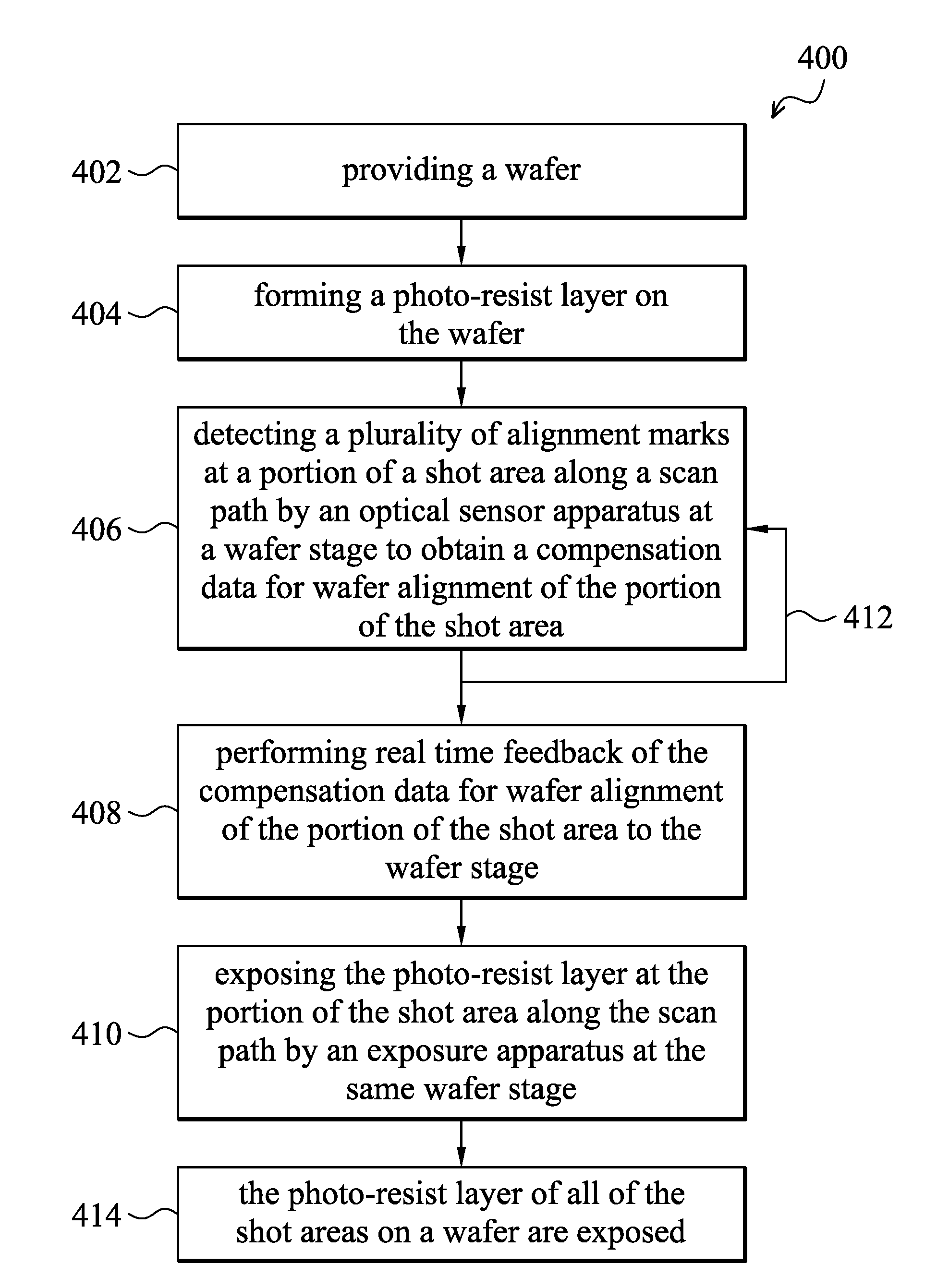
[0016]The following description is of the best-contemplated mode of carrying out the invention. This description is made for the purpose of illustrating the general principles of the invention and should not be taken in a limiting sense. The scope of the invention is best determined by reference to the appended claims.

[0017]FIG. 1 is a schematic side view of an exposure scanner system 200 according to an embodiment of the invention. The exposure scanner system 200 includes an exposure apparatus 202, an optical sensor apparatus 204 including a plurality of alignment mark sensors 209, disposed on two opposite sides of the exposure apparatus 202, and a single wafer stage 206 disposed under the exposure apparatus 202. In the exposure scanner system 200, the exposure apparatus 202 and the optical sensor apparatus 204 have the same scan path 203. The wafer stage 206 has a movement path 208 opposite to the scan path 203. A wafer 100 having a photo-resist layer (not shown) formed thereon is...


PUM


Abstract

A dynamic wafer alignment method and an exposure scanner system are provided. The exposure scanner system having a scan path, includes an exposure apparatus, an optical sensor apparatus and a wafer stage. The method comprises the steps of: (a) providing a wafer, having a plurality of shot areas, wherein each shot area has a plurality of alignment marks thereon; (b) forming a photo-resist layer on the wafer; (c) detecting the alignment marks at a portion of a shot area along the scan path by the optical sensor apparatus to obtain compensation data for wafer alignment of the portion of the shot area; (d) performing real time feedback of the compensation data for wafer alignment to the wafer stage; (e) exposing the photo-resist layer at the portion of the shot area along the scan path; (f) continuously repeating the steps (c) to (e) at the shot area along the scan path until all of the photo-resist layer at the shot area are exposed; and (g) repeating the step (f) until the photo-resist layer of all of the shot areas on the wafer are exposed.

Description

BACKGROUND OF THE INVENTION[0001]1. Field of the Invention[0002]The present invention relates to a wafer alignment method, and in particular relates to a dynamic wafer alignment method in an exposure scanner system.[0003]2. Description of the Related Art[0004]During the semiconductor fabrication process, many exposure process steps require a wafer to be aligned in a certain orientation, such that an overlap accuracy of the patterns of each layer on the wafer can be achieved. The wafer used in the exposure process is generally provided with alignment marks thereon to indicate reference orientation positions of the patterns of a certain layer on the wafer.[0005]A wafer has a plurality of shot areas, wherein one shot area is defined by an exposure region on the wafer with a photo mask through an exposure process. An exposure equipment typically performs the exposure process by irradiating light on a photo-resist layer overlying the wafer. The exposure equipment includes an exposure hea...

Claims


Application Information

Patent Timeline
Patent Type & Authority Applications(United States)
IPC IPC(8): G03B27/42
CPCH01L23/544G03F9/7088G03F9/7003H01L2223/54453H01L2924/0002
Inventor CHIU, CHUI-FUSHIH, CHIANG-LIN
Owner NAN YA TECH
Why Eureka
Try Eureka