

Layout versus schematic error system and method
a schematic error and layout technology, applied in the field of schematic design, can solve the problems of difficult to assess the netlist in terms of circuit design, the inability to quickly understand and fix the error, and the inability to consider the lvs error
- Summary
- Abstract
- Description
- Claims
- Application Information
AI Technical Summary
Problems solved by technology
Method used
Image

Examples
Embodiment Construction
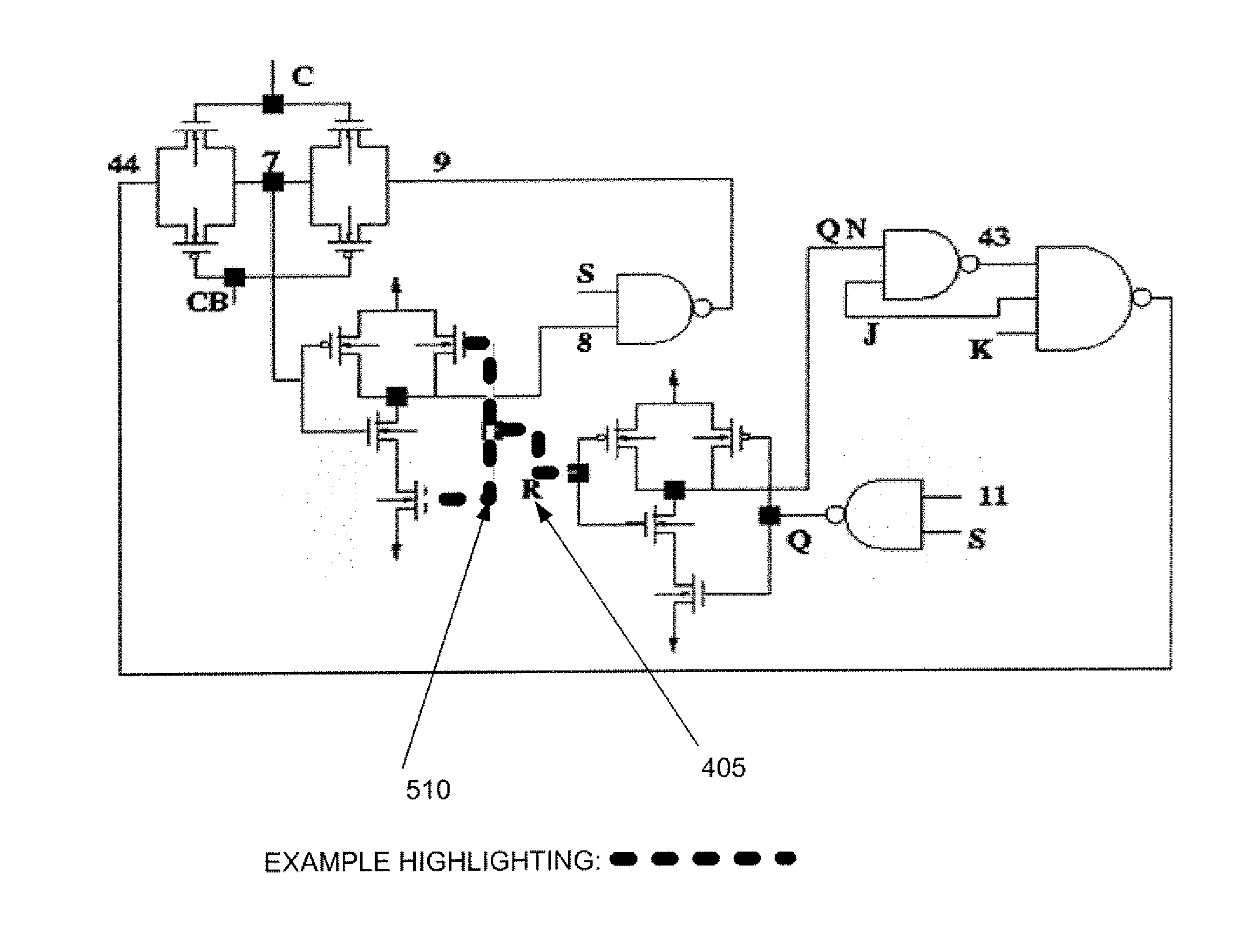
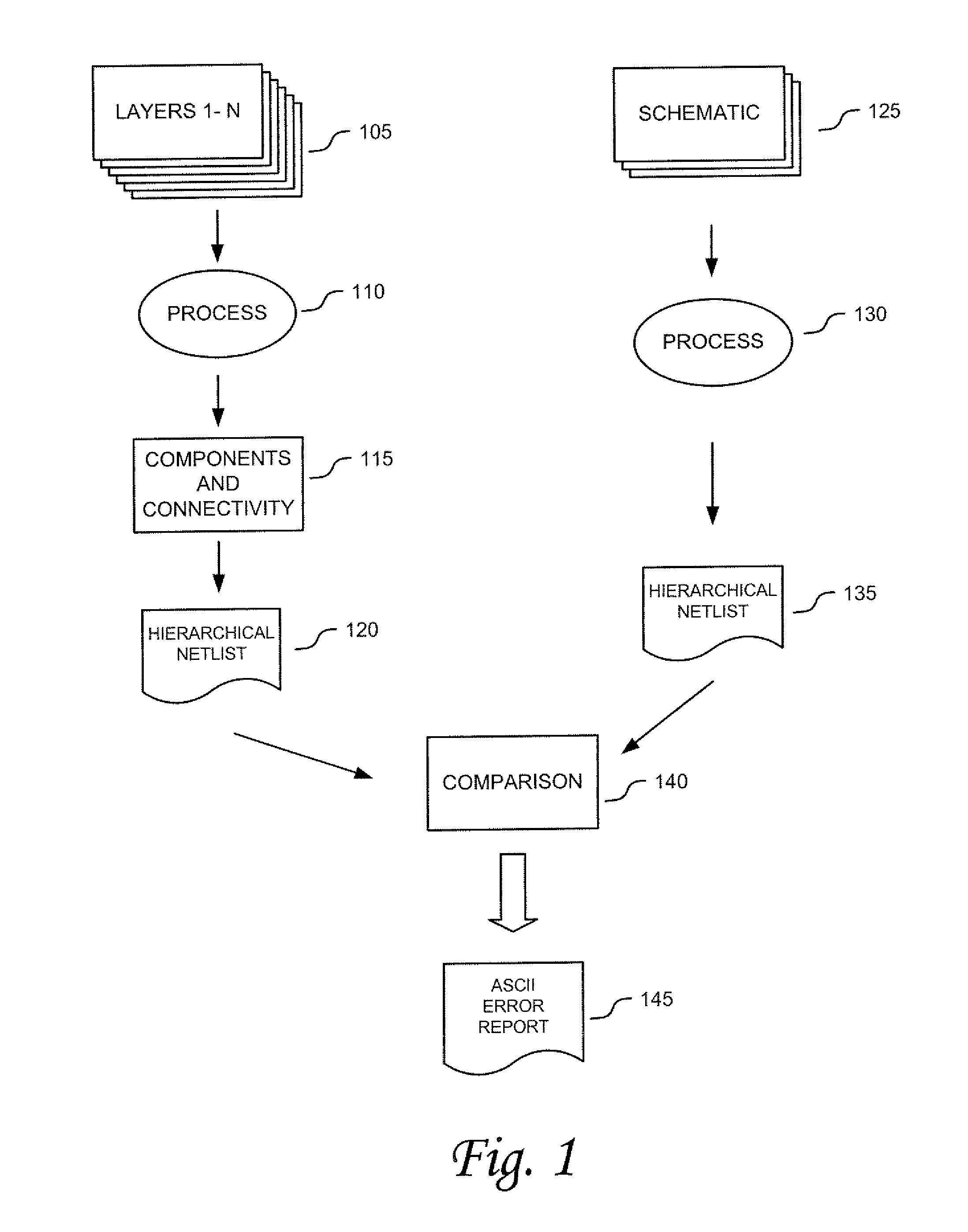
[0010]According to various embodiments of the invention, systems and methods for presenting Layout Versus Schematic (LVS) errors within a layout using a visual circuit representation of the design and highlighting is provided. One embodiment includes overlaying the layout circuit representation on the schematic circuit representation with highlighting that indicates the LVS errors. The method of such an embodiment compares a layout netlist against a schematic netlist in order to identify the layout-versus-schematic errors, generates a graphical circuit representation of the layout netlist and a graphical circuit representation of the schematic netlist, displays an overlay of a graphical representation of the layout netlist with the graphical representation of the schematic netlist, and, then, highlights the identified layout-versus-schematic errors that are present.
[0011]In another embodiment, a method and a tool used to identify layout-versus-schematic errors is provided. The metho...
PUM
 Abstract
Description
Claims
Application Information