Method of Manufacturing Dummy Gates in Gate Last Process

Active Publication Date: 2013-03-07
INST OF MICROELECTRONICS CHINESE ACAD OF SCI
View PDF52 Cites 34 Cited by
  • Summary
  • Abstract
  • Description
  • Claims
  • Application Information

AI Technical Summary

Benefits of technology

[0007]Therefore, the object of the present invention is to provide a method of manufacturing a dummy gate in a g

Problems solved by technology

Such rectangular gate trenches with a large aspect ratio and a small size present great challenges to th

Method used


Image

  • Method of Manufacturing Dummy Gates in Gate Last Process
  • Method of Manufacturing Dummy Gates in Gate Last Process
  • Method of Manufacturing Dummy Gates in Gate Last Process

Examples


Embodiment Construction

[0021]The features and technical effects of the technical solution of the present invention will be described in detail below with reference to the drawings and in conjunction with the exemplary embodiments, and a method of manufacturing a dummy gate in a gate last process is disclosed. It shall be noted that like reference signs indicate like structures.

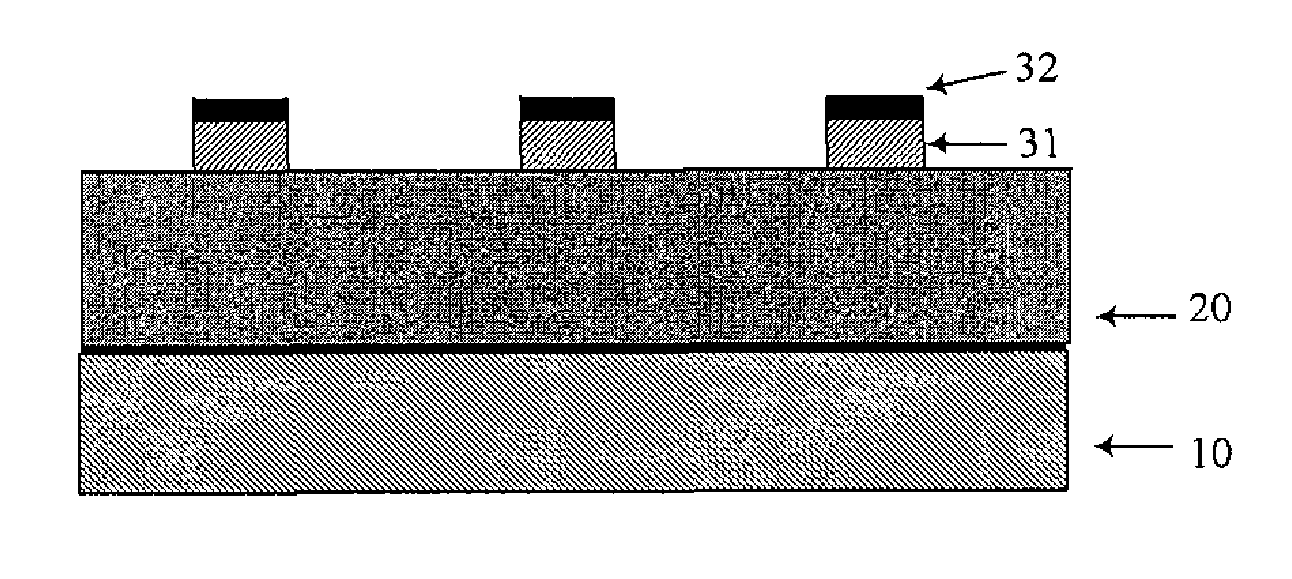
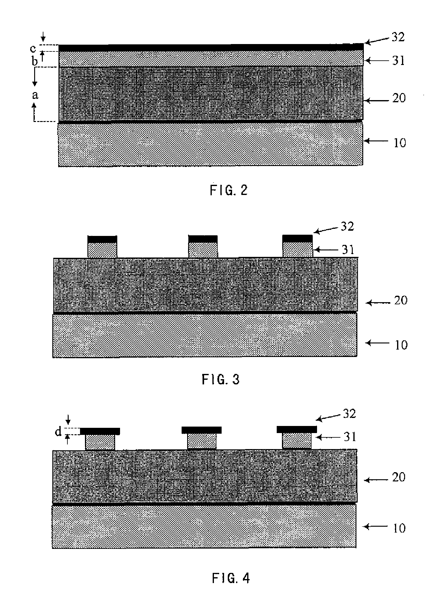
[0022]First, referring to FIG. 2, a dummy gate material layer 20 and a hard mask material layer 30 comprising a first mask layer 31 and a second mask layer 32 are deposited sequentially on a substrate 10 by, for example, LPCVD and PECVD. According to the electrical properties of the device, the substrate 10 may include, for example, bulk silicon, Silicon-On-Insulator (SOI), monocrystalline germanium, and / or Germanium-On-Insulator (GeOI), or other compound semiconductor materials such as SiGe, SiC, InSb, GaAs and GaN. The dummy gate material layer 20 may comprise materials having different etching selectivity from the materials of th...


PUM


Abstract

The present invention provides a method of manufacturing a dummy gate in a gate last process, which comprises the steps of forming a dummy gate material layer and a hard mask material layer sequentially on a substrate; etching the hard mask material layer to form a top-wide-bottom-narrow hard mask pattern; dry etching the dummy gate material layer using the hard mask pattern as a mask to form a top-wide-bottom-narrow dummy gate. According to the dummy gate manufacturing method of the present invention, instead of vertical dummy gates used conventionally, top-wide-bottom-narrow trapezoidal dummy gates are formed, and after removing the dummy gates, trapezoidal trenches can be formed. It facilitates the subsequent filling of the high-k or metal gate material and enlarges the window for the filling process; as a result, the device reliability will be improved.

Description

CROSS-REFERENCE[0001]This application is a National Stage Application of, and claims priority to, PCT Application No. PCT / CN2011 / 002001, filed on Nov. 30, 2011, entitled “Method of Manufacturing Dummy Gates in Gate Last Process”, which claims priority to Chinese Application No. 201110257658.7, filed on Sep. 1, 2011. Both the PCT application and the Chinese application are incorporated herein by reference in their entireties.FIELD OF THE INVENTION[0002]The present invention relates to a method of manufacturing a semiconductor device, more particularly to a method of manufacturing a dummy gate in a gate last process.BACKGROUND OF THE INVENTION[0003]The success of high-k metal-gate (HKMG) in the 45 nm technology node has made it key to the process flow for the sub-30 nm technology node. Intel, who has committed to a metal-gate-last approach, is now the leader in mass production of 45 nm and 32 nm chips. And former IBM alliances such as Sumsung, TSMC and Infineon have recently switched ...

Claims


Application Information

Patent Timeline
IPC IPC(8): H01L21/336
CPCH01L29/66545H01L21/28114H01L21/32139H01L21/31111H01L29/51
Inventor YANG, TAOZHAO, CHAOYAN, JIANGLI, JUNFENGLU, YIHONGCHEN, DAPENG
Owner INST OF MICROELECTRONICS CHINESE ACAD OF SCI
Why Eureka
Try Eureka