RF shielding for electronic components

a technology for electronic components and shielding, applied in the field of electronic product assembly, can solve the problems of faulty components that must first be exposed, reduce the space that would otherwise be available for components, and faulty components to achieve the effect of easy breakage of joints

Inactive Publication Date: 2013-05-16
APPLE INC
View PDF9 Cites 30 Cited by
  • Summary
  • Abstract
  • Description
  • Claims
  • Application Information

AI Technical Summary

Benefits of technology

[0010]In some other embodiments, there may be provided an assembly that may include a first portion configured to be attached to a mounting surface, a second portion removably coupled to the first portion, and a third portion configured to be attached to the first portion once the second portion is removed for shielding a component on the mounting surface. In some embodiments, for example, at least one of the first portion, the second portion, and the third portion may include RF opaque material. In some embodiments, for example, the second portion may be removably coupled to the first portion at an easily broken joint. In some embodiments, for example, the third portion may be configured to be welded to the first portion. In some embodiments, for example, the first portion may include a top and at least one side extend

Problems solved by technology

However, if the functional testing fails, then it may be necessary to remove the faulty component (if that is in fact what is causing the failure) or at least provide access to the faulty component.
Unfortunately, in order to release, or rework, the faulty co

Method used


Image

  • RF shielding for electronic components
  • RF shielding for electronic components
  • RF shielding for electronic components

Examples


Embodiment Construction

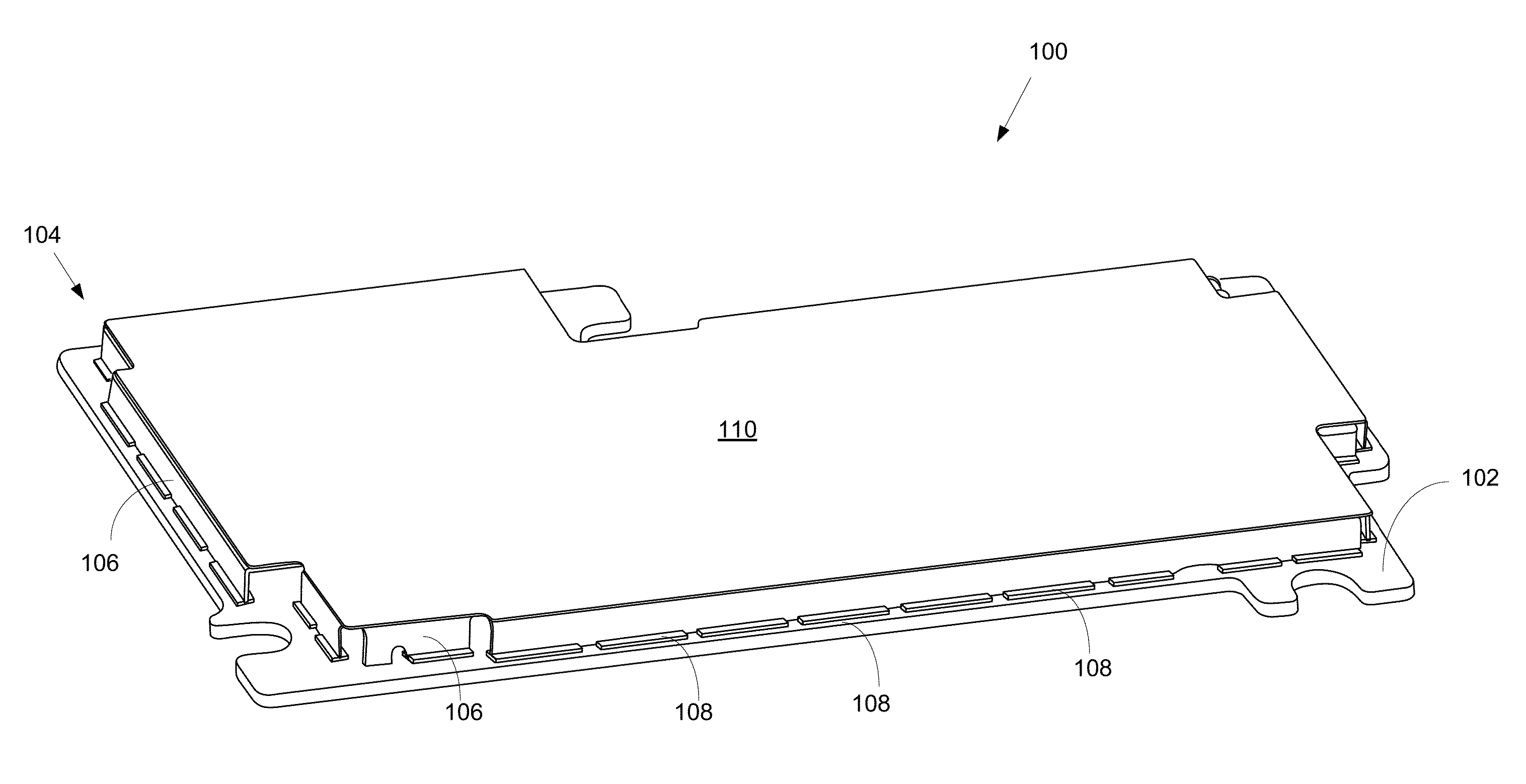
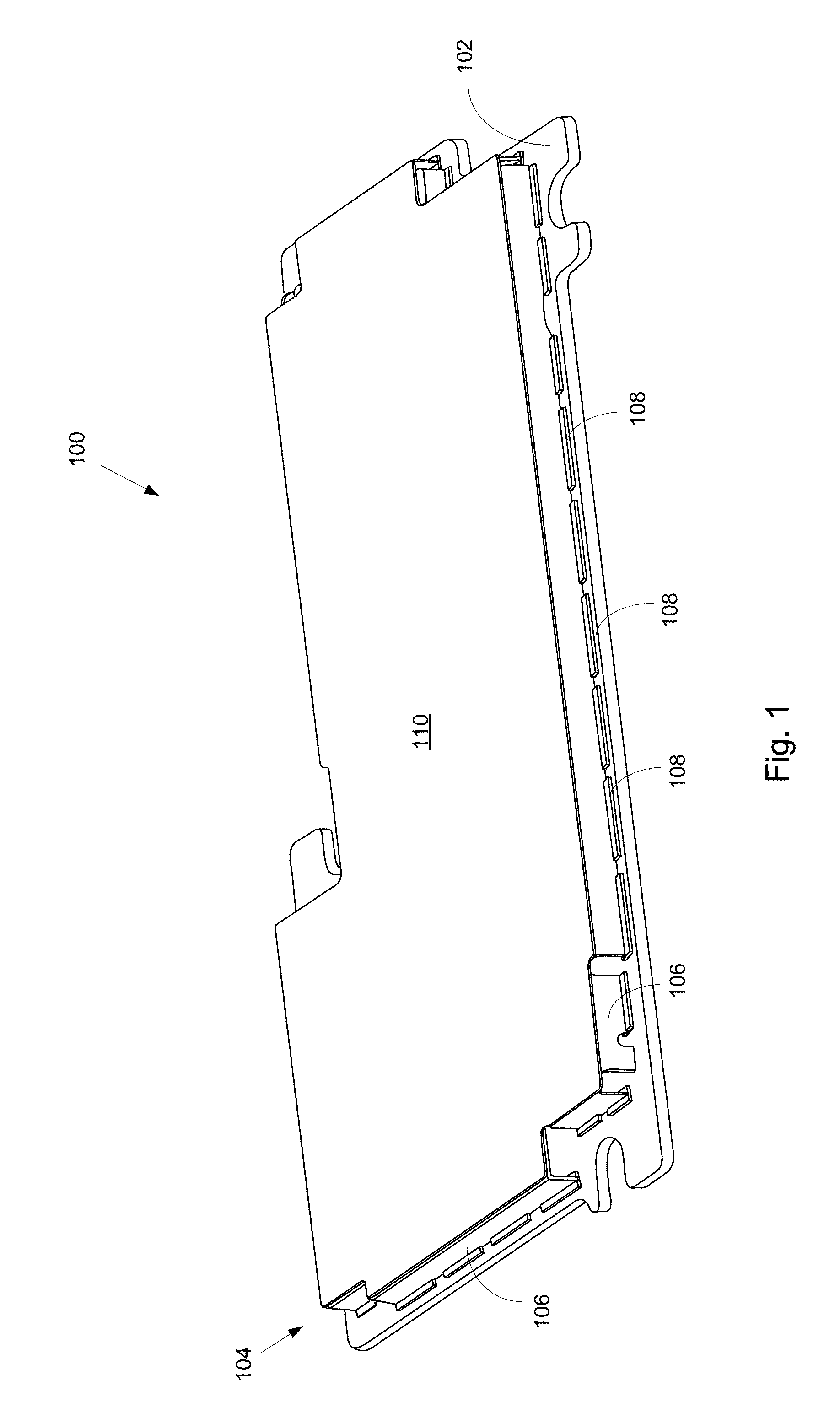
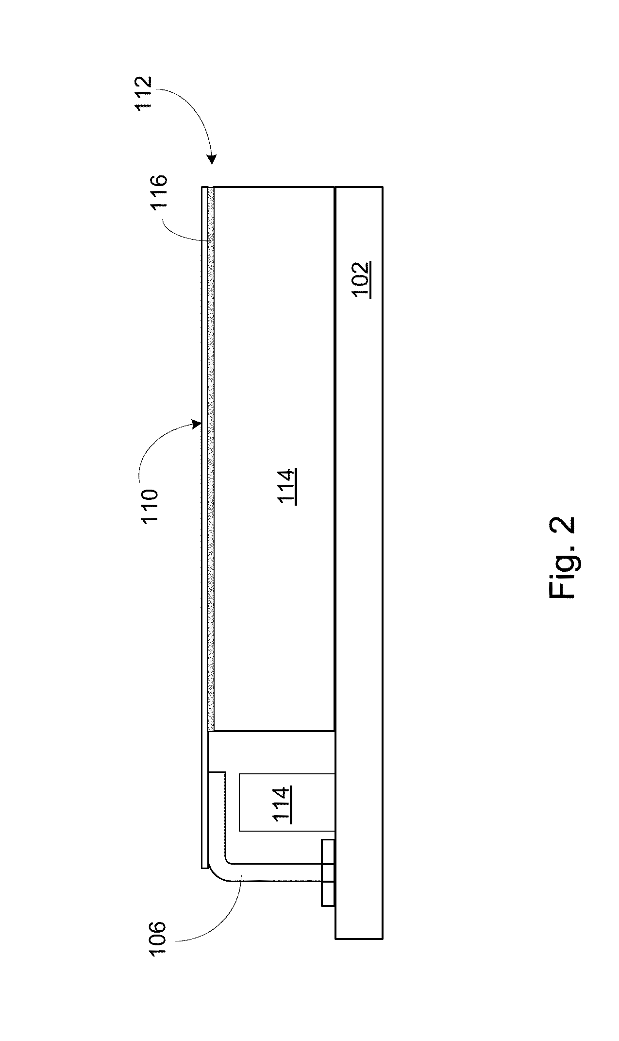
[0006]An RF shield formed of RF opaque material that permits access to components on a printed circuit board (PCB), the RF shield attached to the PCB and enclosing a portion of the PCB on which is mounted at least one electronic component, the enclosed portion of the PCB being RF isolated is described. The RF shield includes at least a fence secured to the PCB and a reduced thickness lid conductively attached to the fence. In the described embodiment, the reduced thickness lid includes at least a layer of metal having a thickness in a range of about 0.009 or 0.010 millimeters to 0.050 millimeters, wherein a clearance between a bottom surface of the layer of metal and at the least one electronic component is within a range of 0.0 millimeters to about 0.010 millimeters. The layer of metal can be aluminum, copper, and so forth.

[0007]In another embodiment, a method of assembly is described. The method of assembly is carried out by performing at least the following operations: providing ...


PUM

PropertyMeasurementUnit
Lengthaaaaaaaaaa
Lengthaaaaaaaaaa
Lengthaaaaaaaaaa

Abstract

An RF shield formed of RF opaque material that permits access to components on a printed circuit board is described. The RF shield can include a first portion attached to the PCB and a removable top portion attached to the first portion at an interface. The top portion is removed from the first portion to expose the components on the PCB. In one aspect of the described embodiment, the top portion is peeled away from the first portion. The components are enclosed within the RF shield after the removal of the top portion by attaching and sealing another top portion to the first portion at the interface by, for example, laser attaching the first portion and the other top portion at the interface.

Description

CROSS-REFERENCE TO RELATED APPLICATIONS[0001]This application claims the benefit of prior filed U.S. Provisional Patent Application No. 61 / 559,865, filed Nov. 15, 2011, and of prior filed U.S. Provisional Patent Application No. 61 / 563,464, filed Nov. 23, 2011, each of which is incorporated by reference herein in its entirety.TECHNICAL FIELD[0002]The present invention relates generally to assembly of electronic products. More particularly, a method and an apparatus are described for providing radio frequency (RF) shielding for electronic components soldered to or otherwise attached to a printed circuit board, or PCB. Specific embodiments describe a low profile RF shielding structure some of which can provide for defective component rework.BACKGROUND OF THE INVENTION[0003]During the assembly of many electronic products, various components must be attached to a printed circuit board. Generally, the components are attached at contact pads that act as both a support structure and an elec...

Claims


Application Information

Patent Timeline
IPC IPC(8): H05K9/00H05K3/34H05K3/30
CPCH05K9/0032H05K1/0216H05K3/225H05K2201/1031Y10T29/49133H05K2203/176Y10T29/49144Y10T29/4913H05K2201/10371Y02P70/50
Inventor WERNER, CHRISTOPHER MATTHEWROTHKOPF, FLETCHER R.LYNCH, STEPHEN BRIANPYPER, DENNIS R.CHEN, WYEMANNIKKHOO, MICHAEL M.SALEHI, AMIR
Owner APPLE INC
Why Eureka
Try Eureka