Semiconductor device

a semiconductor and display device technology, applied in semiconductor devices, digital storage, instruments, etc., can solve the problems of difficult to prolong a period, difficult to increase the driving frequency of the driver circuit, and charge leaked from the gate of the transistor mb>1/b>, so as to achieve the effect of reducing the w/l of the transistor

Active Publication Date: 2013-06-06
SEMICON ENERGY LAB CO LTD
View PDF2 Cites 19 Cited by
  • Summary
  • Abstract
  • Description
  • Claims
  • Application Information

AI Technical Summary

Benefits of technology

[0016]Embodiments of the present invention can provide a driver circuit that can operate even at high driving frequencies, provide a driver circuit that ...

Problems solved by technology

Consequently, it is difficult to increase the driving frequency of the driver circuit in Patent Document 1.
However, charge is leaked from the gate of the transistor M1 because of the off-state current of a transistor whose source or drain is connected to the gate of the transistor M1.
It is therefore difficult to prolong a period du...

Method used


Image

  • Semiconductor device
  • Semiconductor device
  • Semiconductor device

Examples


embodiment 1

[0040]In this embodiment, a basic circuit, a sequential circuit including the basic circuit, and a shift register circuit including the sequential circuit which are embodiments of the present invention will be described.

[0041]First, the configuration of a basic circuit in this embodiment will be described with reference to FIG. 1A.

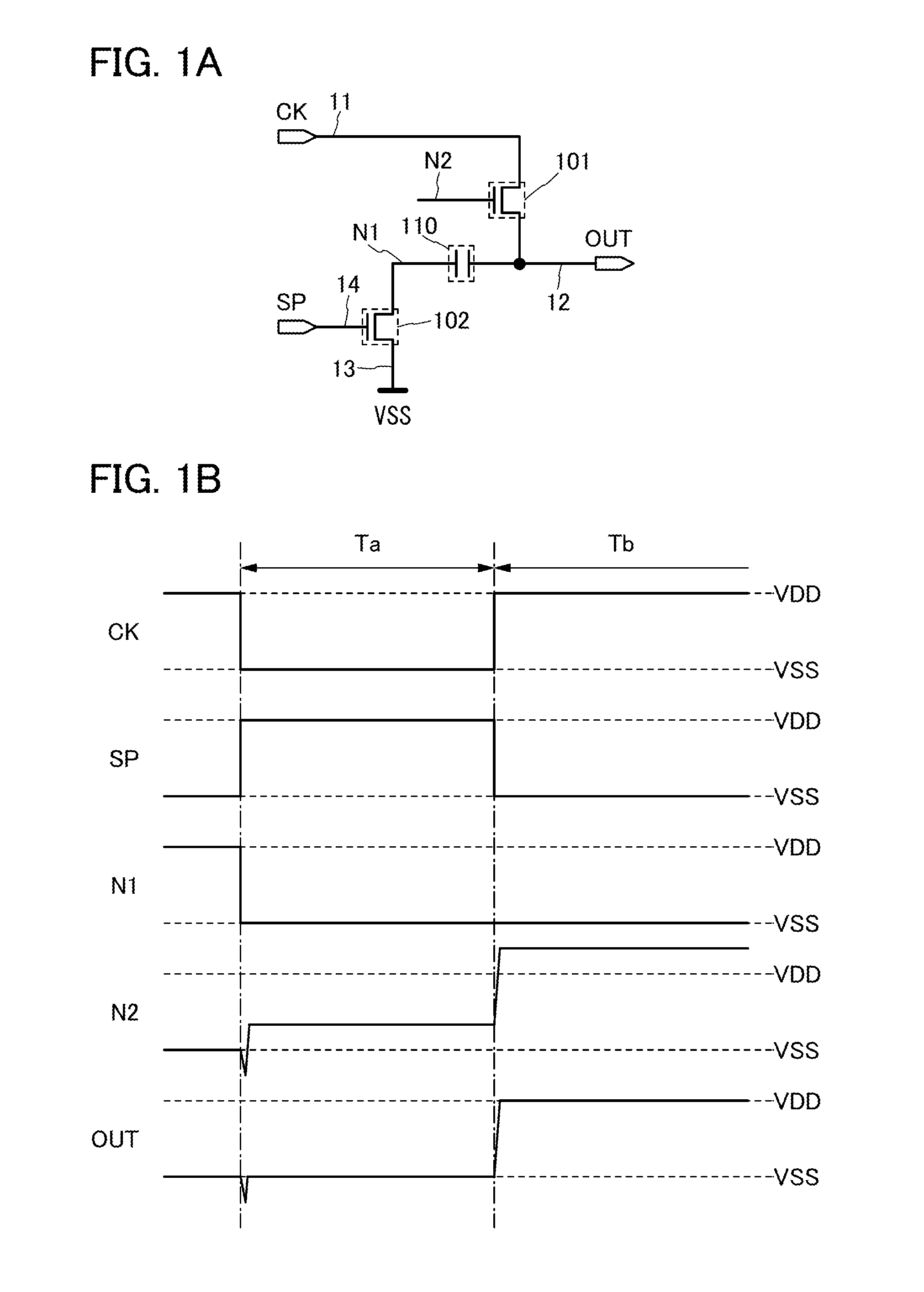
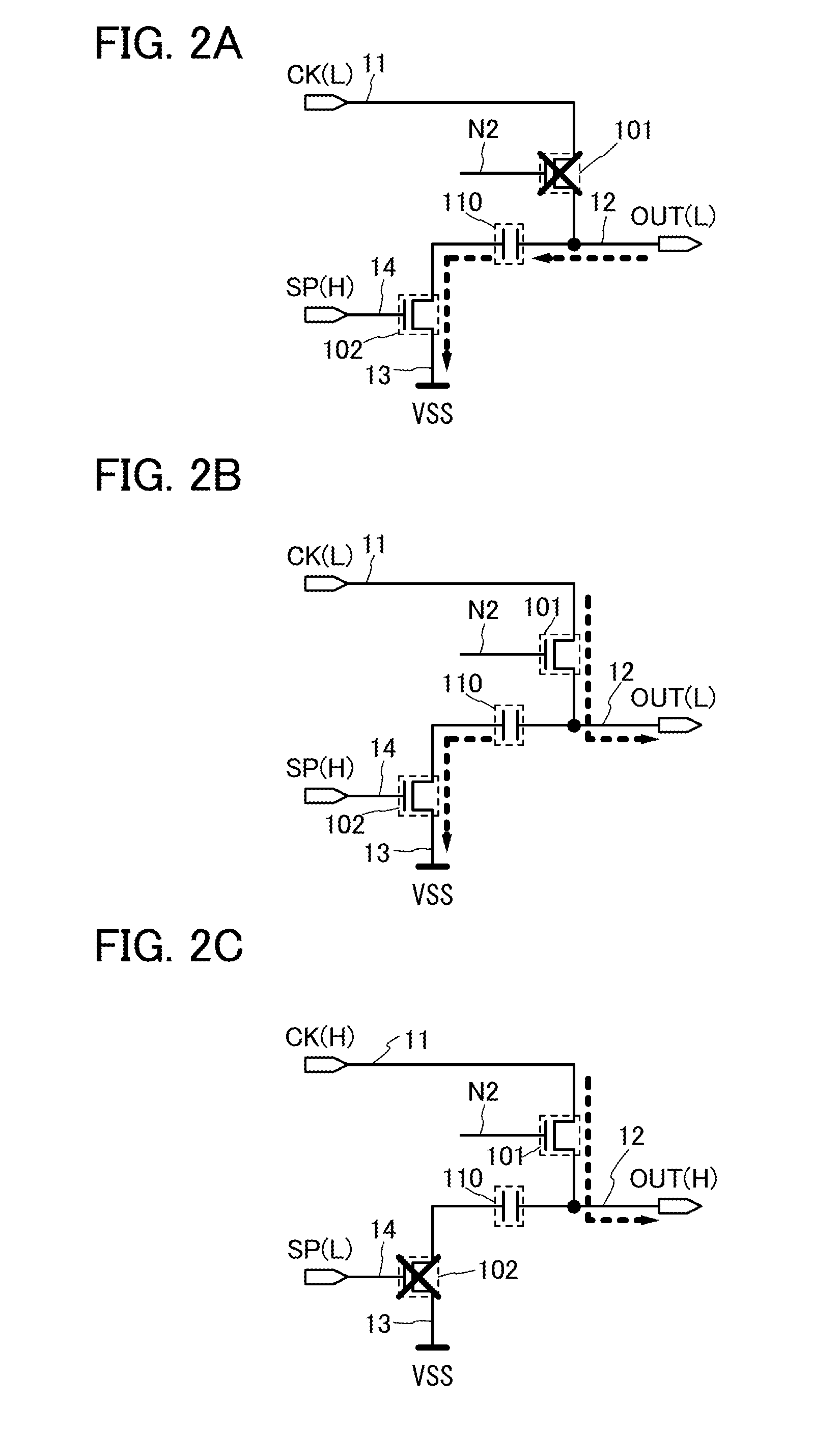
[0042]The basic circuit in FIG. 1A includes a transistor 101, a transistor 102, and a capacitor 110.

[0043]A first terminal of the transistor 101 is connected to a wiring 11. A second terminal of the transistor 101 is connected to a wiring 12.

[0044]A first terminal of the transistor 102 is connected to a wiring 13. A gate of the transistor 102 is connected to a wiring 14.

[0045]A first electrode (also referred to as one electrode) of the capacitor 110 is connected to the wiring 12. A second electrode (also referred to as the other electrode) of the capacitor 110 is connected to a second terminal of the transistor 102.

[0046]Note that the second terminal of th...

embodiment 2

[0121]In this embodiment, a basic circuit including a buffer circuit and a sequential circuit including the basic circuit will be described.

[0122]First, the configuration of a basic circuit in this embodiment will be described with reference to FIG. 6A. The basic circuit in FIG. 6A has a configuration in which a transistor 201 is provided in the basic circuit in FIG. 1A.

[0123]Note that the transistor 201 preferably has the same conductivity type as the transistor 101. In this embodiment, the case where these transistors are n-channel transistors will be described.

[0124]A first terminal of the transistor 201 is connected to the wiring 11. A second terminal of the transistor 201 is connected to a wiring 31. A gate of the transistor 201 is connected to the gate of the transistor 101.

[0125]The transistor 201 has a function of controlling electrical continuity between the wiring 11 and the wiring 31, a function of supplying the signal CK of the wiring 11 to the wiring 31, and a function ...

embodiment 3

[0157]In this embodiment, sequential circuits different from those in Embodiments 1 and 2 will be described.

[0158]A sequential circuit in FIG. 7A has a configuration in which the second terminal of the transistor 105 is connected to the wiring 16 in the sequential circuit in FIG. 3.

[0159]In the sequential circuit in FIG. 7A, the wiring 15 and the potential VDD can be omitted.

[0160]Note that in any of the sequential circuits and the shift register circuit described in Embodiments 1 and 2, the second terminal of the transistor 105 may be connected to the wiring 16.

[0161]A sequential circuit in FIG. 7B has a configuration in which the second terminal of the transistor 105 in the sequential circuit in FIG. 3 is connected to a wiring 17.

[0162]The wiring 17 (also referred to as signal line) is supplied with a signal CKB and has a function of transmitting or supplying the signal CKB. The signal CKB is a signal having high and low levels. The signal CKB corresponds to one of a plurality of ...


PUM


Abstract

A semiconductor device capable of high-speed operation. The semiconductor device includes a first transistor, a second transistor, and a capacitor. One of a source and a drain of the first transistor is supplied with a first signal. One of a source and a drain of the second transistor is supplied with a first potential. A gate of the second transistor is supplied with a second signal. A first electrode of the capacitor is electrically connected to the other of the source and the drain of the first transistor. A second electrode of the capacitor is electrically connected to the other of the source and the drain of the second transistor. In a first period, the first signal is low and the second signal is high. In a second period, the first signal is high and the second signal is either low or high.

Description

BACKGROUND OF THE INVENTION[0001]1. Field of the Invention[0002]One embodiment of the present invention relates to semiconductor devices, display devices, and the like.[0003]2. Description of the Related Art[0004]The increase in size of display devices such as liquid crystal display devices and EL display devices promotes the development of display devices with higher added value. In particular, techniques by which a driver circuit in a display device is composed of only transistors having the same conductivity type have been actively developed (see Patent Document 1).[0005]FIG. 16 illustrates a driver circuit disclosed in Patent Document 1. The driver circuit in Patent Document 1 includes transistors M1 to M7. When a signal GOUT[N−1] goes high, the transistor M3 is turned on. Thus, a voltage VON is supplied to a gate of the transistor M1, so that the gate potential of the transistor M1 starts to rise. Since the gate potential of the transistor M1 rises gradually, a potential differ...

Claims


Application Information

Patent Timeline
IPC IPC(8): H01L27/07
CPCH01L27/0733G11C19/184G11C19/28G09G3/3266H01L27/1255G09G2310/0286G09G2320/043H01L27/124H01L27/1251G09G2310/0267
Inventor UMEZAKI, ATSUSHI
Owner SEMICON ENERGY LAB CO LTD
Why Eureka
Try Eureka