
Faraday Shield Having Plasma Density Decoupling Structure Between TCP Coil Zones

a plasma density and shielding technology, applied in the field of semiconductor fabrication, can solve the problems of adversely affecting the throughput of wafers interfering with the etching process, etc., and achieve the effect of better plasma density control

Active Publication Date: 2013-07-25
LAM RES CORP
View PDF10 Cites 11 Cited by
  • Summary
  • Abstract
  • Description
  • Claims
  • Application Information

AI Technical Summary

Benefits of technology

The invention is a Faraday shield that is placed inside a chamber to protect the window through which plasma is applied to a wafer during a chemical etching process. The shield has two zones separated by a band ring, which allows for independent control of the magnetic field distribution. The shield also has radial slots that enable precise plasma density control across the wafer surface. This improves the uniformity of plasma density and helps to protect the dielectric window from plasma byproduct buildup. Overall, the invention provides better plasma density control and protects the chamber components from damage during etching operations.

Problems solved by technology

Adherence of non-volatile reaction products to the window may interfere with the etching process.
Excessive deposition may result in particles flaking off the window onto the wafer, thus interfering with the etching process.
Excessive deposition, therefore, requires more frequent cleaning of the chamber walls and the window which adversely affects wafer throughput.
Additionally, if the window becomes coated with etch byproducts, the ability of the chamber transmit sufficient magnetic flux to the plasma becomes diminished, which in turn reduces the ability to control the directionality of etch operations, which are critical when processing high aspect ratio profile features.

Method used


Image

  • Faraday Shield Having Plasma Density Decoupling Structure Between TCP Coil Zones
  • Faraday Shield Having Plasma Density Decoupling Structure Between TCP Coil Zones
  • Faraday Shield Having Plasma Density Decoupling Structure Between TCP Coil Zones

Examples


Embodiment Construction

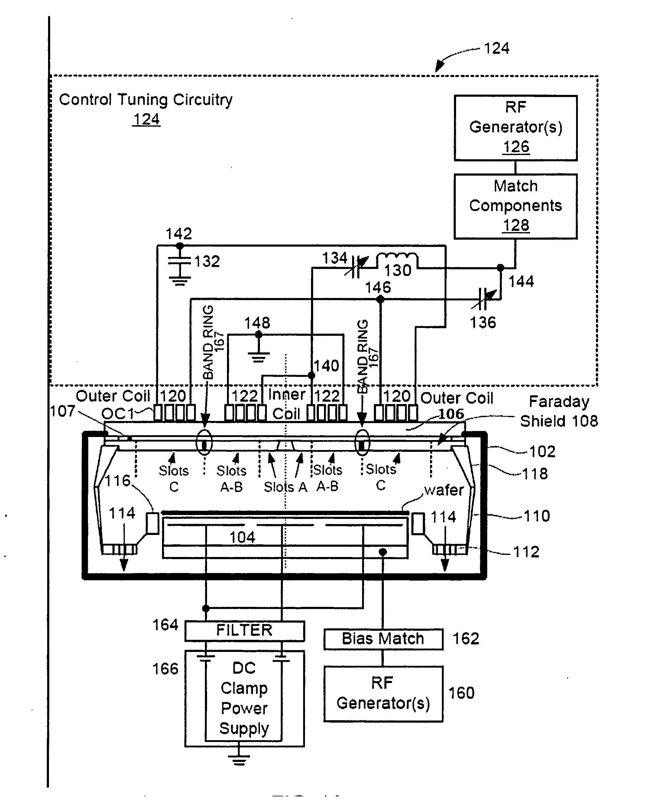
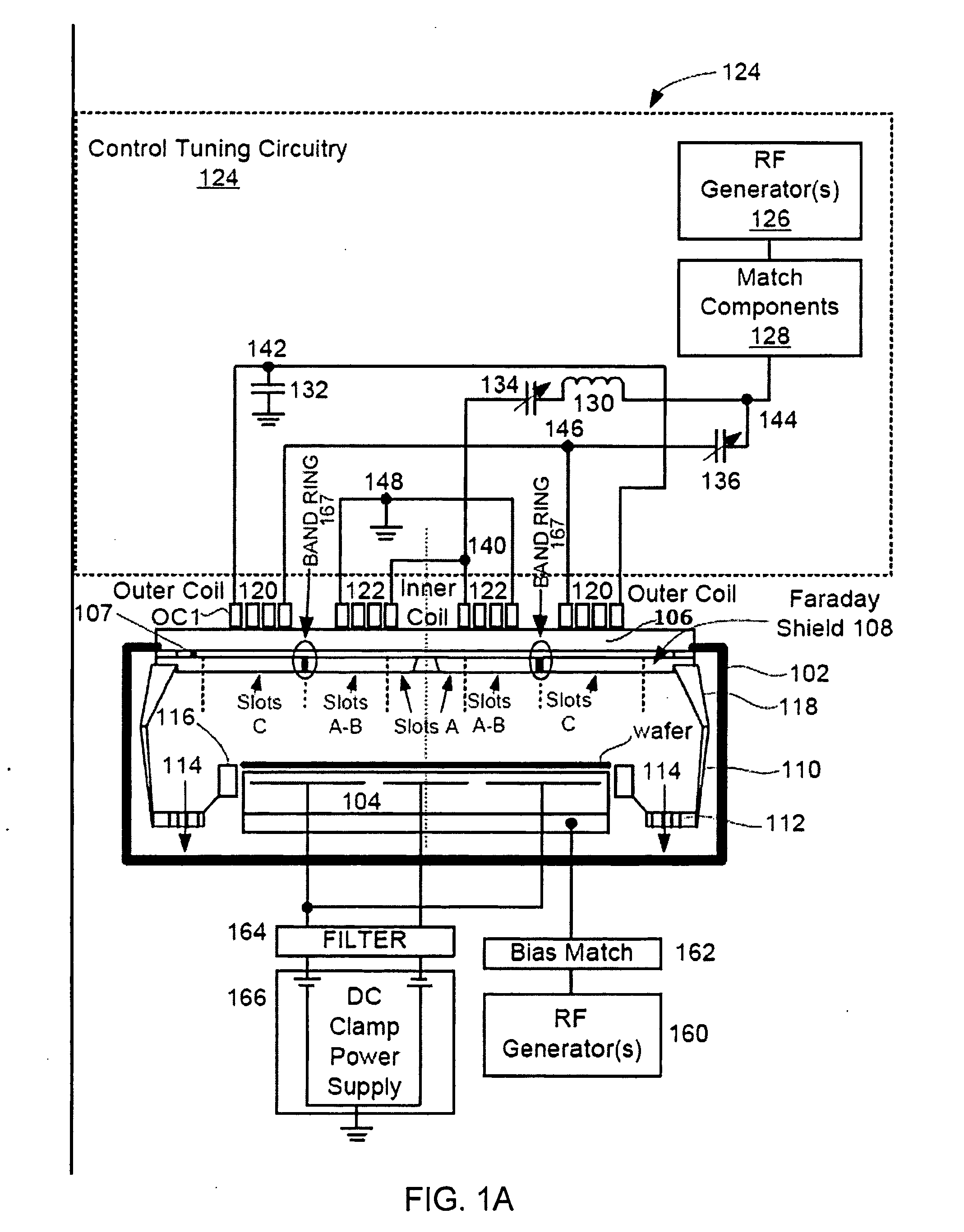
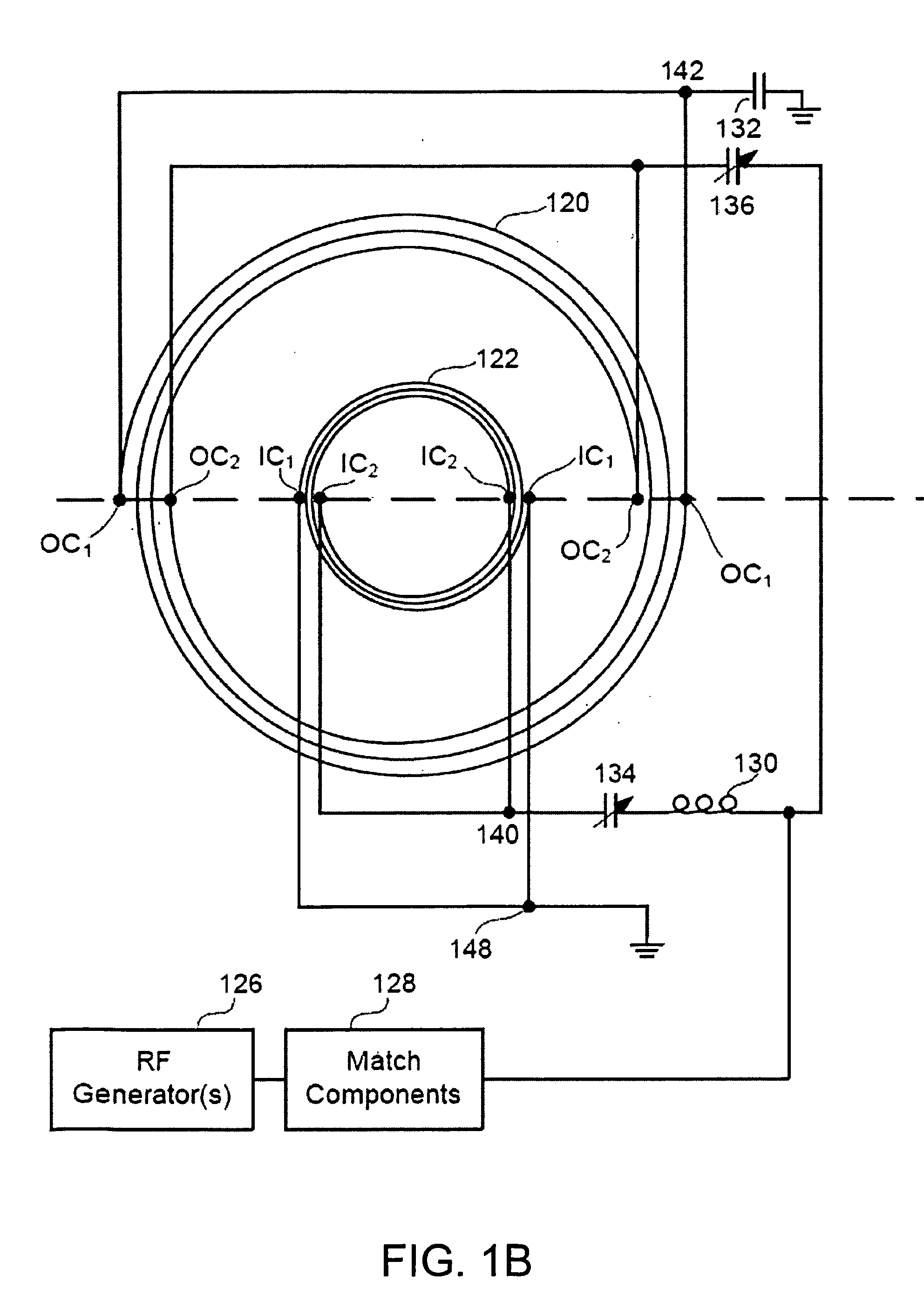
[0025]Disclosed is an apparatus used in etching semiconductor substrates and layers formed thereon during the manufacture of semiconductor devices. The apparatus is defined by a chamber in which etching is performed. A Faraday shield is disposed within the chamber, and is configured with a three zone slot configuration that is correlated to the placement of a TCP coil disposed over a dielectric window of the chamber.

[0026]In one embodiment, the Faraday shield includes a band ring that is used to physically separate slot openings in an inner region of the Faraday shield from slot openings in an outer region of the Faraday shield. The band ring, in one embodiment, provides for improved decoupling control of the applied magnetic flux imparted by the inner and outer coils, respectively. The band ring is a plasma density decoupling structure, that is integral to the Faraday shield. The decoupling provides for an improved tuning knob, which may be used to achieve desired etch uniformities...


PUM

PropertyMeasurementUnit
Lengthaaaaaaaaaa
Lengthaaaaaaaaaa
Lengthaaaaaaaaaa

Abstract

A Faraday shield and a plasma processing chamber incorporating the Faraday shield is are provided. The plasma chamber includes an electrostatic chuck for receiving a substrate, a dielectric window connected to a top portion of the chamber, the dielectric window disposed over the electrostatic chuck, and a Faraday shield. The Faraday shield is disposed inside of the chamber and defined between the electrostatic chuck and the dielectric window. The Faraday shield includes an inner zone having an inner radius range that includes a first and second plurality of slots and an outer zone having an outer radius range that includes a third plurality of slots. The inner zone is adjacent to the outer zone. The Faraday shield also includes a band ring separating the inner zone and the outer zone, such that the first and second plurality of slots do not connect with the third plurality of slots.

Description

PRIORITY CLAIM[0001]This application claims priority as a Continuation-in-Part of U.S. patent application Ser. No. 13 / 198,683, filed on Aug. 4, 2011, and entitled “Internal Faraday Shield Having Distributed Chevron Patterns and Correlated Positioning Relative to External Inner and Outer TCP Coil, which claims priority to U.S. Provisional Patent Application No. 61 / 480,314 filed on Apr. 28, 2011 and entitled “Internal Faraday Shield Having Distributed Chevron Patterns and Correlated Positioning Relative to External Inner and outer TCP Coil,” all of which are incorporated herein by reference in their entirety for all purposes.FIELD OF THE INVENTION[0002]The present invention relates generally to semiconductor fabrication, and more particularly, to an apparatus containing a Faraday shield for improving etch chamber plasma uniformity.DESCRIPTION OF THE RELATED ART[0003]In semiconductor manufacturing, etching processes are commonly and repeatedly carried out. As is well known to those ski...

Claims


Application Information

Patent Timeline
IPC IPC(8): H01L21/67H05K9/00
CPCH01J37/32651H05K9/00H01L21/67069
Inventor LONG, MAOLINPATERSON, ALEXMARSH, RICKYWU, YINGDREWERY, JOHN
Owner LAM RES CORP
Learn More