
Variable resistive memory device and method of fabricating and driving the same

Active Publication Date: 2013-08-29
SK HYNIX INC
View PDF5 Cites 24 Cited by
  • Summary
  • Abstract
  • Description
  • Claims
  • Application Information

AI Technical Summary

Benefits of technology

The patent describes a variable resistive memory device with multiple memory cells arranged in rows and columns. The device includes a common wiring electrically connected to the memory cells, a selection device for selecting a specific memory cell, and a common selection line for applying a common reference voltage and operating voltage to the memory cells. The device also includes first and second insulated gate structures independently controlled by a selection voltage for selecting a specific memory cell. The method of driving the device involves applying a common reference voltage and operating voltage, and selectively applying a selection voltage to the selected memory cell to swing its threshold voltage. The device and method provide efficient and reliable programming of the memory cells.

Problems solved by technology

However, since flash memories require a relatively high capacity transistor in order to perform hot carrier injection for programming and a tunneling oxide film that is thick enough to endure a high internal voltage in order to ensure reliable data retention, there is a basic limitation in scaling down flash memories.

Method used


Image

  • Variable resistive memory device and method of fabricating and driving the same
  • Variable resistive memory device and method of fabricating and driving the same
  • Variable resistive memory device and method of fabricating and driving the same

Examples


Embodiment Construction

[0042]The present invention will now be described more fully with reference to the accompanying drawings, in which exemplary embodiments of the invention are shown.

[0043]Hereinafter, the present invention will be described more fully with reference to the accompanying drawings, in which exemplary embodiments of the invention are shown. The invention may, however, be embodied in many different forms and should not be construed as being limited to the embodiments set forth herein; rather these embodiments are provided so that this disclosure will be thorough and complete, and will fully convey the concept of the invention to one of ordinary skill in the art.

[0044]In the drawings, the same reference numerals denote the same elements. As used herein, the term “and / or” includes any and all combinations of one or more of the associated listed items.

[0045]The terminology used herein is for the purpose of describing particular embodiments only and is not intended to be limiting of exemplary...


PUM


Abstract

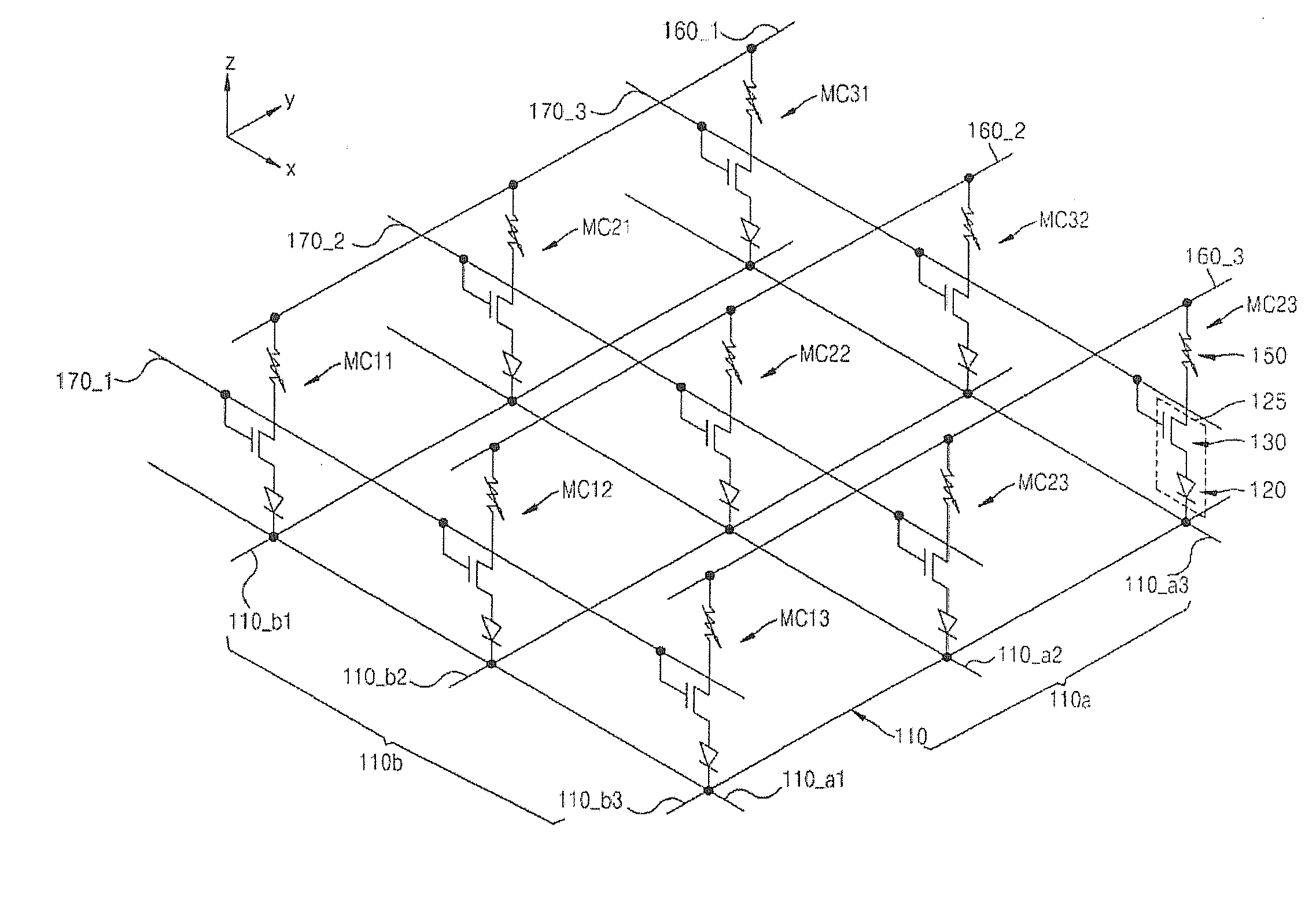
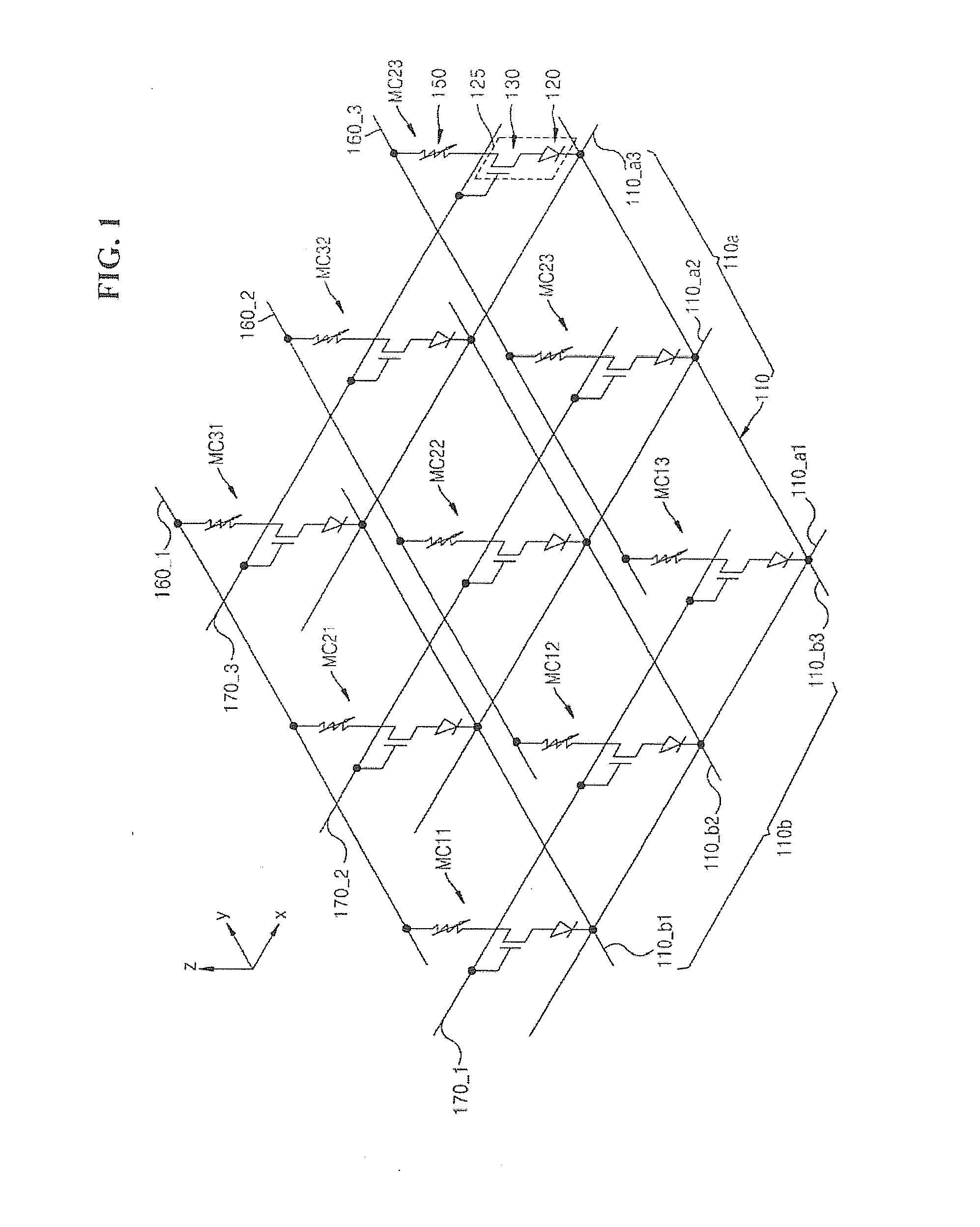
Provided are a variable resistive memory device, and methods of fabricating and driving the same. The variable resistive memory device includes a plurality of memory cells arranged in a first direction and in a second direction different from the first direction, each of the plurality of memory cells comprising a variable resistor and a selection device serially connected to the variable resistor. A common wiring is electrically connected to first ends of the plurality of memory cells to apply a common reference voltage. Each wiring line of a plurality of wiring lines is electrically connected to second ends of the plurality of memory cells arranged n the plurality of rows oriented in the first direction. A plurality of selection lines are respectively connected to the selection devices of the plurality of memory cells to select any one of the plurality of memory cells via the plurality of wiring lines.

Description

CROSS-REFERENCE TO RELATED PATENT APPLICATION[0001]This application claims the benefit of Korean Patent Application No. 10-2012-0014542, filed on Feb. 13, 2012, in the Korean Intellectual Property Office, the disclosure of which is incorporated herein in its entirety by reference.BACKGROUND OF THE INVENTION[0002]1. Field of the Invention[0003]The present invention relates to a memory device, and more particularly, to a variable resistive memory device, and methods of fabricating driving the same.[0004]2. Description of the Related Art[0005]As demands for portable digital application devices such as a digital camera, an MP3 player, a personal digital assistant (PDA), and a mobile phone have increased, the nonvolatile memory market has grown fast. High-density flash memory devices having low fabricating costs per bit are widely used as programmable nonvolatile memories. However, since flash memories require a relatively high capacity transistor in order to perform hot carrier injectio...

Claims


Application Information

Patent Timeline
IPC IPC(8): G11C13/00G11C11/16G11C17/16H01L45/00
CPCH01L45/06G11C13/0016H01L45/1233H01L45/142H01L45/143H01L45/144H01L45/146H01L45/147H01L45/1683H01L27/2436H01L27/2454H01L27/2463H01L27/2481G11C13/0004H01L45/04H01L45/16G11C11/16G11C17/16G11C13/0011H01L45/085G11C11/1659G11C11/1657H10B63/34H10B63/84H10B63/30H10B63/80H10N70/245H10N70/20H10N70/8822H10N70/8825H10N70/8836H10N70/231H10N70/066H10N70/8828H10N70/8833H10N70/826H10B63/20H10N70/011
Inventor PARK, NAM KYUNDO, GAP SOK
Owner SK HYNIX INC
Learn More