Data latch circuit, driving method of the data latch circuit, and display device

a data latch and driving method technology, applied in the field of data latch circuits, can solve the problems of increasing the expansion of the circuit scale and the increase of power consumption, increasing the power consumption, so as to reduce the dependence on the threshold voltage, operate stably, and reduce power consumption

Inactive Publication Date: 2011-04-19
SEMICON ENERGY LAB CO LTD
View PDF27 Cites 25 Cited by
  • Summary
  • Abstract
  • Description
  • Claims
  • Application Information

AI Technical Summary

Benefits of technology

[0017]By having such a circuit structure, it is possible to operate the inverter with power source voltage. Therefore, in this circuit structure, through current which has flowed to a conventional inverter can be reduced and the dependency on threshold voltage is less than before. Thus, a circuit hardly affected by a variation in TFT characteristics, with lower power consumption, and being able to operate stably can be provided.
[0018]A data latch circuit of the present invention has a circuit structure in which only two potentials of VDD and VSS are applied in a holding portion even though the amplitude of an input signal is smaller than the amplitude of a drive power source. By having such a circuit structure, it is possible to reduce power consumption because through current can be reduced, and to carry out operation certainly without being affected by the variation in the TFT characteristics. Moreover, since boosting with an external circuit is not necessary, it is possible to decrease the power consumption, the layout area, and the cost.

Problems solved by technology

However, a data latch circuit corresponding to low signal voltage input causes an error by variation in TFT characteristics, particularly variation in the threshold.
Moreover, although the data latch circuit responds to such an error by increasing the amplitude of a signal with the use of a level conversion circuit or the like in accordance with drive voltage of an internal circuit, additional use of such a level conversion circuit or the like increases the expansion of a circuit scale and the increase in power consumption.
If a video signal with small amplitude is held in a data latch circuit without any change, through current flows to a logic element in a data holding portion, thereby increasing the power consumption.

Method used


Image

  • Data latch circuit, driving method of the data latch circuit, and display device
  • Data latch circuit, driving method of the data latch circuit, and display device
  • Data latch circuit, driving method of the data latch circuit, and display device

Examples


embodiment modes

Embodiment Mode 1

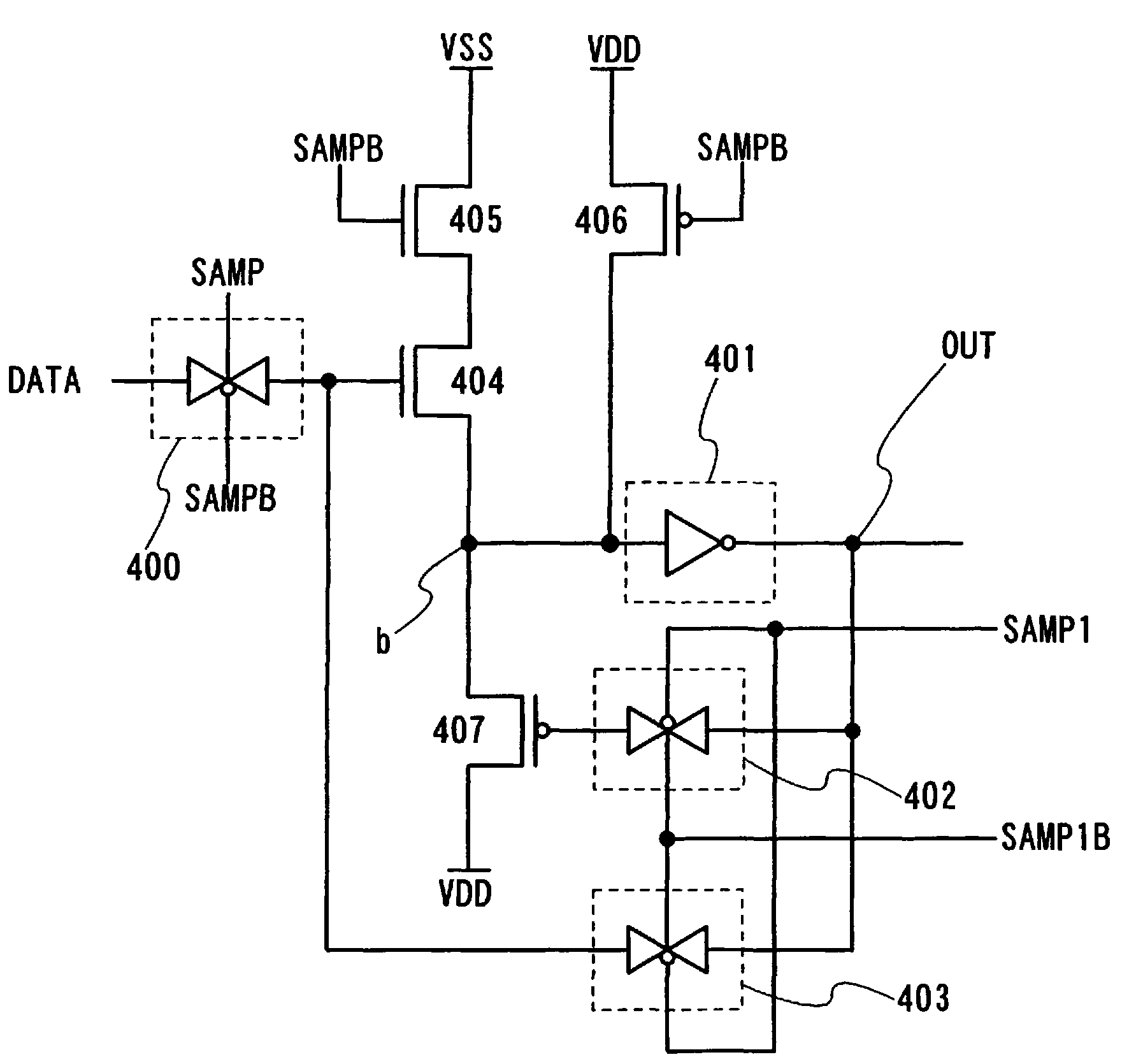
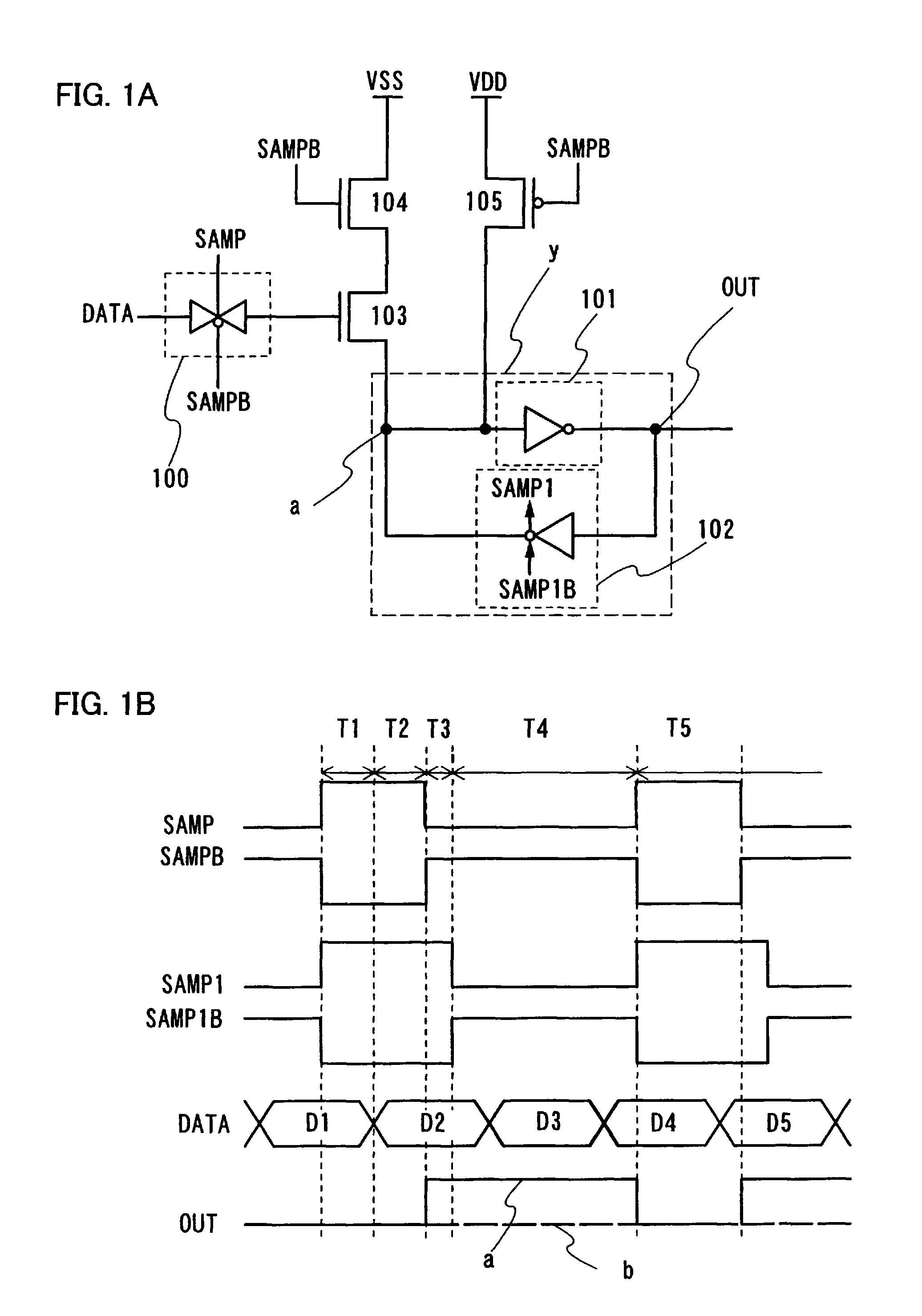
[0035]An embodiment mode of the present invention is hereinafter described with reference to the drawings. In the description of this embodiment mode, the following parameters are used for convenience. It is to be noted that the parameters shown here are one drive condition for a circuit of the present invention, and another combination of different parameters is also allowed as long as a similar operational effect to that in this embodiment mode can be obtained. As a drive power source of the circuit, VSS=0 V and VDD=5 V (5 Vpp) are used. The amplitudes of a sampling (SAMP) signal and an inverted sampling (SAMPB) signal are set at a high (H) level of 5 V and a low (L) level of 0 V (5 Vpp). The amplitudes of a sampling 1 (SAMP1) signal and an inverted sampling 1 (SAMP1B) signal are set at a high (H) level of 5 V and a low (L) level of 0 V (5 Vpp). The amplitude of a data (DATA) signal is set at a high (H) level of 3.3 V and a low (L) level of 0 V (3.3 Vpp). As for T...

embodiment mode 2

[0063]This embodiment mode will describe an example of using the data latch circuit employed in this embodiment mode in a source signal line driver circuit. The source signal line driver circuit is to sample a data signal to be inputted and output a signal which has been analog-converted to a source line corresponding to a pixel to be driven.

[0064]FIG. 5 shows an example of a structure of a source signal line driver circuit. The source signal line driver circuit often includes a shift register 600, a latch circuit 601, and a D / A converting circuit (Digital / Analog Converter: DAC) 602. Usually, in the source signal line driver circuit, some level shifters are additionally needed to amplify a data signal when operating the latch circuit; however, the level shifters are not necessary in the present invention. The source lines with the number corresponding to the number of rows of pixels are necessary in the actual source driver; therefore, a source driver portion in a display device inc...

embodiment mode 3

[0068]This embodiment mode will describe, with reference to FIGS. 6A and 6B, a display device including the data latch circuit shown in Embodiment Modes 1 and 2, of which a display screen is formed by applying to a pixel a light-emitting element using a material expressing electroluminescence.

[0069]In FIG. 6A, a display panel 1501 has a pixel portion 1503 including a plurality of pixels 1502 arranged in matrix. Each pixel 1502 has a switching element such as a TFT and a light-emitting element connected thereto. A connection wire 1508 which connects an external circuit 1507 and the display panel 1501 may have driver ICs mounted, which form a signal line driver circuit 1505 and a scan line driver circuit 1506. The data latch circuit shown in Embodiment Modes 1 and 2 is incorporated in the driver IC.

[0070]As another mode, the signal line driver circuit 1505 and the scan line driver circuit 1506 can be provided over a substrate where the pixel portion 1503 is formed, as shown in FIG. 6B...


PUM


Abstract

The present invention provides a data latch circuit which can operate stably with a low-amplitude signal, which consumes less electric power, and which is resistant against the variation in TFTs.When an analog switch is turned on, a data signal is inputted to a gate electrode of an n-channel TFT and, at this time, VDD is supplied to an input terminal of an inverter. When the analog switch in turned off, the n-channel TFT is turned on or off depending on a level of the data signal. When the data signal is at an H level, the n-channel TFT is turned on and VSS is supplied to the input terminal of the inverter. When the data signal is at an L level, VDD is supplied to an input terminal of the inverter. Therefore, only VDD and VSS levels are applied to the input terminal of the inverter.

Description

BACKGROUND OF THE INVENTION[0001]1. Field of Invention[0002]The present invention relates to a data latch circuit for sampling and holding a signal at a desired timing. In particular, the present invention relates to, in an active matrix display device for displaying an image with the use of a digital image signal, a data latch circuit for sampling and holding the digital image signal. Moreover, the present invention relates to an electronic appliance using an active matrix display device having a driver circuit including the data latch circuit.[0003]2. Description of the Related Art[0004]In recent years, techniques for forming a thin film transistor (TFT) over an insulating substrate have drastically progressed, and development of a flat panel display typified by a liquid crystal display device or the like has been promoted in view of the increase in demand of flat panel displays for mobile appliances. In particular, development of techniques for integrally forming a pixel portion ...

Claims


Application Information

Patent Timeline
Patent Type & Authority Patents(United States)
IPC IPC(8): G09G3/36G06F3/038G09G5/00H03L5/00
CPCG09G3/20G09G3/3275G09G3/2022G09G3/3258G09G3/3266H03K3/356147G09G2300/0861G09G2310/027G09G2310/0294G09G2330/021G09G2300/0842G02F1/13G02F1/133G09G3/36
Inventor OSAME, MITSUAKIUENO, TATSURO
Owner SEMICON ENERGY LAB CO LTD
Why Eureka
Try Eureka