
Reducing write amplification in a flash memory

a technology of flash memory and write amplification, which is applied in the field of flash memory, can solve the problems of shortening the life span of flash memory and reducing sustained performance, and achieve the effect of reducing write amplification

Active Publication Date: 2013-09-05
AVAGO TECH INT SALES PTE LTD
View PDF2 Cites 61 Cited by
  • Summary
  • Abstract
  • Description
  • Claims
  • Application Information

AI Technical Summary

Benefits of technology

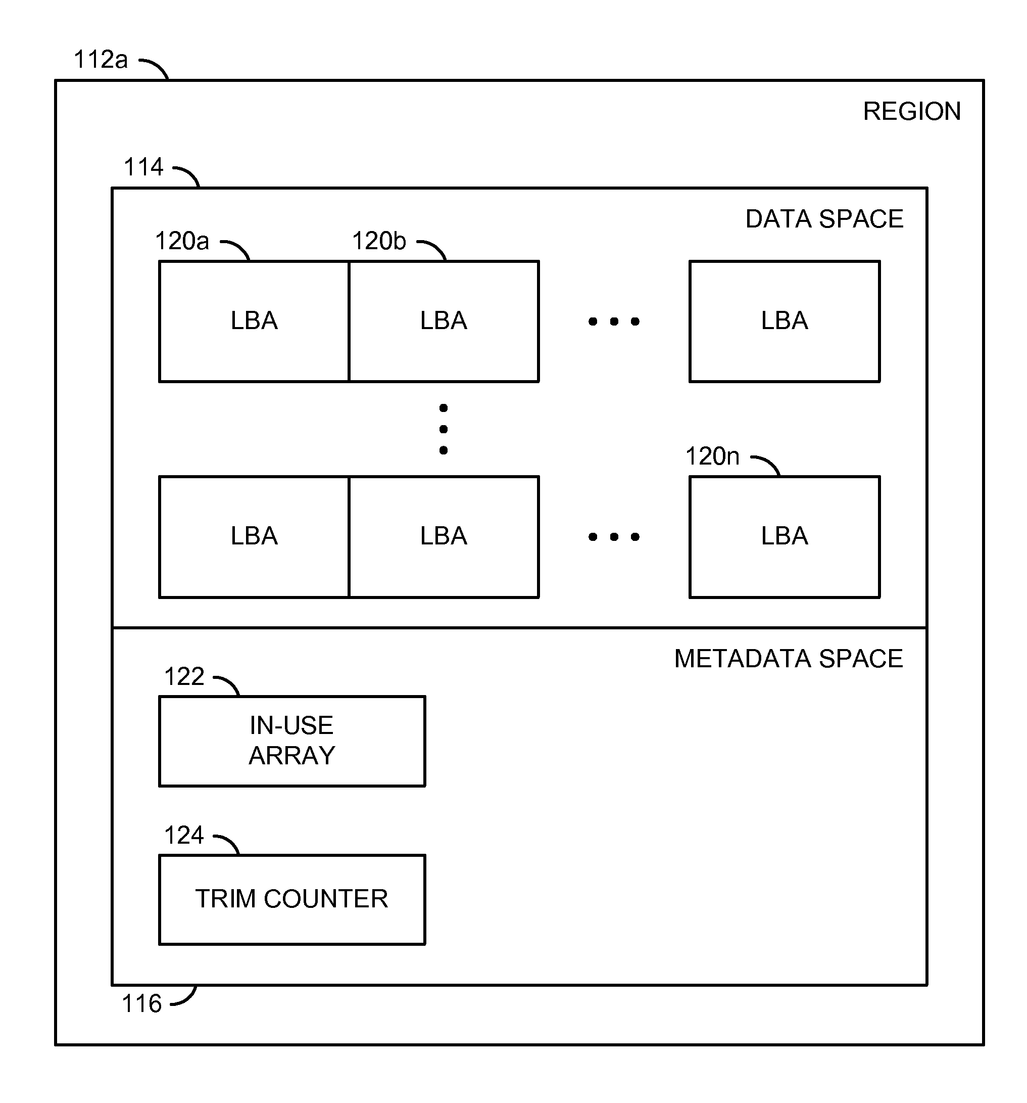
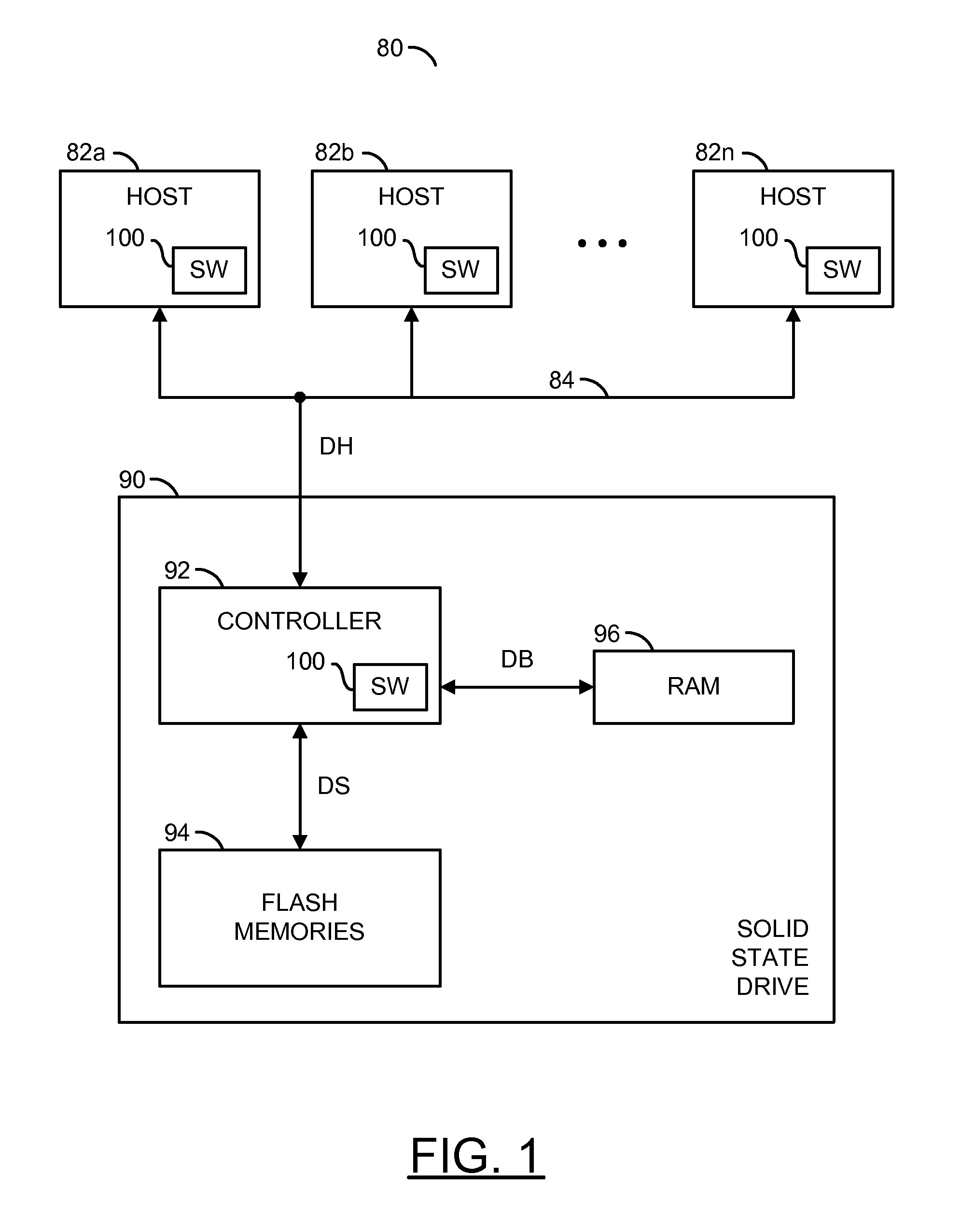
The present invention is about a device with a memory circuit and a manager. The memory circuit has Flash memories and a space that spans multiple memory addresses. The manager receives data from applications in random order and stores it in a specific region of the memory circuit. The data items have their own host address and can be written without affecting each other. This minimizes the amount of data that needs to be written, which is important for reducing write amplification. The invention can provide a near-performance ratio for Flash memory and can be used with solid-state drives. Additionally, it can track free / used information on a per-region basis.

Problems solved by technology

Higher numbers for the write amplification results in shorter life spans of the FLASH memories and lower sustained performances.

Method used


Image

  • Reducing write amplification in a flash memory
  • Reducing write amplification in a flash memory
  • Reducing write amplification in a flash memory

Examples


Embodiment Construction

[0016]Boolean logical NAND-based Flash memories (or devices) may move data around in a background to even out the usage of pages within the Flash memories. The background movement generally extends a limited life of the devices (e.g., limited number of writes each device may support). To even out the usage, Flash memories may re-map a write to either (i) a new unused location or (ii) a lesser used location when the write is received from a server (e.g., a host computer). To create available spaces, movement of some data is designed to create regions and blocks of contiguous space.

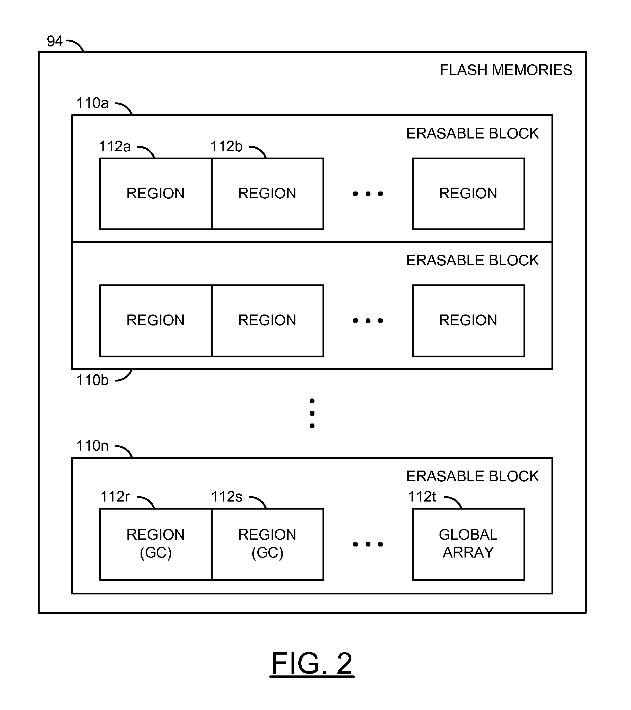
[0017]A NAND Flash memory may be written in units of pages and erased in units of blocks. One or more blocks may be treated as a large erase block with a range from approximately 1 gigabyte (e.g., GB) up to 16 GB in size. Each erase block may also be divided into multiple regions. A size of each region generally ranges from approximately 512 megabytes (e.g., MB) to 4 GB. For example, an erase block of 4 GB ...


PUM


Abstract

An apparatus having a memory circuit and a manager is disclosed. The memory circuit generally has (i) one or more Flash memories and (ii) a memory space that spans a plurality of memory addresses. The manager may be configured to (i) receive data items in a random order from one or more applications, (ii) write the data items in an active one of a plurality of regions in a memory circuit and (iii) mark the memory addresses in the active region that store the data items as used. Each data item generally has a respective host address. The applications may be executed in one or more computers. The memory addresses in the active region may be accessed in a sequential order while writing the data items to minimize a write amplification. The random order is generally preserved between the data items while writing in the active region.

Description

FIELD OF THE INVENTION[0001]The present invention relates to Flash memory generally and, more particularly, to a method and / or apparatus for reducing write amplification in a Flash memory.BACKGROUND OF THE INVENTION[0002]Conventional NAND Flash memories move data in the background to write over an entire span uniformly. The background data movement is called wear leveling. A process performing the background data movement is often referred to as a garbage collection process. Since Flash memories only write in increments of a page (i.e., 4 kilobytes (KB), 8 KB or 16 KB) and erase data in terms of blocks (i.e., 64 KB up to 512 KB), the background data movement prolongs a useful life and performance of the device. A ratio of a number of writes that happen within the Flash memories per each write received from the user is called a write amplification. Higher numbers for the write amplification results in shorter life spans of the FLASH memories and lower sustained performances.[0003]It ...

Claims


Application Information

Patent Timeline
IPC IPC(8): G06F12/00
CPCG06F2212/7205G06F12/0246
Inventor ISH, MARKPANDA, SIDDHARTHA K.
Owner AVAGO TECH INT SALES PTE LTD
Learn More