
Multi-chip package

a technology of multi-chips and chips, applied in the field of semiconductor packages, can solve the problems of substrates being likely to short circuit, increase the thickness of the package, and incurred a lot of costs, and achieve the effects of compactness, compactness and miniaturization, and light weigh

Active Publication Date: 2014-01-16
SK HYNIX INC
View PDF0 Cites 7 Cited by
  • Summary
  • Abstract
  • Description
  • Claims
  • Application Information

AI Technical Summary

Benefits of technology

This patent is about a new shape of a multi-chip package that is designed to be lightweight, thin, and compact. This package can be used to achieve miniaturization and will have a unique design.

Problems solved by technology

In order to extend the functionality of a semiconductor device in a wafer state, substantial equipment investment is needed in a wafer manufacturing process, a lot of costs are incurred, and various problems likely to occur in processing should be solved first.
Nevertheless, even in such a multi-chip package, the thickness of the package increases due to the presence of the controller chip stacked on the memory chips, and the wires for connecting the controller chip and the substrate are likely to short-circuit with the wires connected with the memory chips.
Thus, a design is complicated, the size of the package increases, and a fail such as wire sweeping and wire damage is likely to occur in a molding process.

Method used


Image

  • Multi-chip package
  • Multi-chip package
  • Multi-chip package

Examples


Embodiment Construction

[0030]Hereafter, various embodiments will be described in detail with reference to the accompanying drawings.

[0031]It is to be understood herein that the drawings are not necessarily to scale and in some instances proportions may have been exaggerated in order to more clearly depict certain features of the invention.

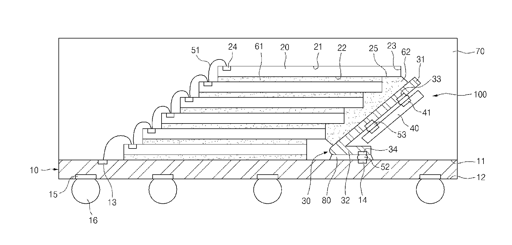
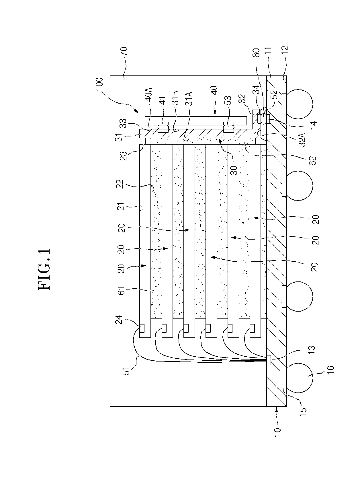
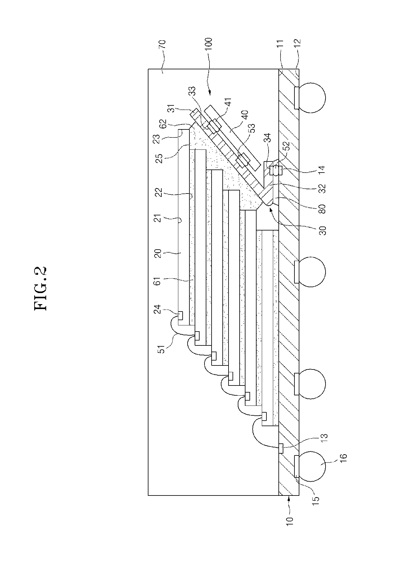
[0032]FIG. 1 is a cross-sectional view illustrating a multi-chip package in accordance with an embodiment.

[0033]Referring to FIG. 1, a multi-chip package in accordance with an embodiment may include a main substrate 10, a plurality of first semiconductor chips 20, and a semiconductor package 100. Additionally, the multi-chip package further may include first and second connection members 51 and 52, first and second adhesive members 61 and 62, a molding part 70, and a fixing member 80.

[0034]The main substrate 10 has an upper surface 11 and a lower surface 12. First connection pads 13 and second connection pads 14 may be formed on the upper surface 11 of the main substrate...


PUM


Abstract

A multi-chip package includes a main substrate; a plurality of first semiconductor chips stacked on an upper surface of the main substrate and having bonding pads which are electrically connected with the main substrate; and a semiconductor package attached to side surfaces of the stacked first semiconductor chips and electrically connected with the main substrate.

Description

CROSS-REFERENCE TO RELATED APPLICATIONS[0001]The present application claims priority U.S.C. 119(a) to Korean Patent Application Number 10-2012-0075576 filed in the Korean Intellectual Property Office on Jul. 11, 2012, which is incorporated herein by reference in its entirety.BACKGROUND[0002]1. Field of the Invention[0003]The present invention generally relates to a semiconductor package, and more particularly, to a multi-chip package which has a novel shape capable of accomplishing light weight, thinness, compactness, and miniaturization.[0004]2. Description of the Related Art[0005]In a semiconductor package, in order to increase capacity and extend functionality, a degree of integration is being gradually increased in a wafer state. Further, a semiconductor package in which at least two kinds of semiconductor chips or semiconductor packages are incorporated is being generalized.[0006]In order to extend the functionality of a semiconductor device in a wafer state, substantial equipm...

Claims


Application Information

Patent Timeline
Patent Type & Authority Applications(United States)
IPC IPC(8): H01L23/538H01L23/495
CPCH01L23/5384H01L23/495H01L23/3128H01L23/49816H01L23/49833H01L23/4985H01L24/73H01L25/065H01L25/0657H01L25/18H01L2224/16145H01L2224/32145H01L2224/48091H01L2224/48145H01L2224/48147H01L2224/48227H01L2224/73204H01L2224/73265H01L2225/0651H01L2225/06527H01L2225/06541H01L2225/06562H01L2225/06572H01L2225/06575H01L2924/181H01L2924/00014H01L2924/00H01L2924/00012H01L23/12H01L23/48
Inventor KIM, KI YOUNGPARK, MYUNG GUN
Owner SK HYNIX INC
Learn More